The market research and strategy consulting company, Yole Développement (Yole), investigates the memory industry for a while. Yole’s analysts combine their technical expertise and knowledge of the semiconductor packaging and memories to deliver a comprehensive overview of the technologies and markets with a dedicated report, titled Memory Packaging. This new study analyzes in detail the challenges and opportunities of the memory packaging industry. It presents an overview of the stand-alone memory markets and provides a valuable understanding of memory packaging technologies and markets.
For Simone Bertolazzi, Ph.D. Senior Market & Technology Analyst, Memory at Yole: “We expect that the overall volume of memory wafers will grow from 35.5 million in 2020 to 50 million in 2026 with a 6% CAGR between 2020 and 2026, while the volume of memory packages will have a 5% CAGR in the same period.”
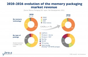
The overall memory packaging market in 2020 is worth US$13.1 billion, which corresponds to about 10% of the stand-alone memory market.
Walt Coon, VP of NAND and Memory Research within the Semiconductor & Software division at Yole, explains:“By 2026, NAND and DRAM revenues are expected to grow with CAGR20-26 of 9% (NAND) and 15% (DRAM), to US$92 billion and US$157 billion, respectively.”
Mike Howard, VP of DRAM and Memory Research within the Semiconductor & Software division at Yole, adds: “In terms of packaging revenues, DRAM is the leading memory technology in 2020 with a 63% share, while wire-bond is the dominant packaging approach being mainly used for mobile applications.”
With the ongoing slowdown of Moore’s Law and the rise of new advanced packaging techniques, back-end processing has gained more and more importance, and several semiconductor companies are now leveraging it – rather than the front-end – to improve the performance, the compactness, and the number of functionalities of their IC products. Heterogeneous integration techniques and chiplet architectures enabled by novel stacking/bonding solutions have become essential to increase the performance of computing systems via a tight integration of logic and memory building blocks.
Memory packaging technologies are also rapidly evolving to meet growing performance needs from data-intensive applications, currently hampered by the so-called “memory wall”, a bandwidth limitation associated with data transfer between memory and processing units. HBM is being commercialized to respond to this challenge, leveraging 3D stacking of DRAM dies using TSVs and thermo-compression bonding.
Nowadays, all memory manufacturers are carrying out R&D activities on hybrid bonding. YMTC was the first player to adopt hybrid bonding for NAND with its Xtacking 3D NAND technology. However, adopting a wafer-to-wafer stacking approach would require a massive conversion of production lines, which is not suitable for companies that already have large production capacity in place. Therefore, analysts expect that incumbent players will continue with their monolithic 3D NAND solutions until the current deck-stacking approach runs out of steam.
Hybrid bonding is widely being explored for next generation HBM devices, and Yole’s memory team believes, it could make its first entry into the market before the next five years. However, significant technical challenges still need to be addressed to achieve high yields suitable for high-volume manufacturing.
















 Back to News