


NexWafe GmbH, today announced completion of a €10 million capital raise with participation from both existing and new shareholders. Pioneers of in-line epitaxy for production of high-efficiency monocrystalline silicon wafers, NexWafe’s EpiWafers provide solar panel manufacturers with dramatically higher efficiency and uncompromised yield at 70 percent of the cost of traditional monocrystalline Cz-Si, all without having to retool their production lines. NexWafe’s technology also allows for production of ultra-thin wafers, already demonstrated in the company’s pilot line in Freiburg, providing a roadmap to next-generation ultra-thin and tandem architectures.
Investors in the Series B round include Fraunhofer, Saudi Aramco Energy Ventures, GAP Technology Holding, Lynwood Schweiz AG and Bantina Invest Limited. With this additional cash infusion, NexWafe will move forward with further industrialization of its EpiNex™ green high-efficiency solar wafer technology and begin its pilot manufacturing activities. As the company moves into its next stage, it is also intensifying discussions with potential partners to commercialize the technology. The company’s CEO, Davor Sutija, has a longstanding track record in creating such partnerships and will be leading this effort. He was appointed to his position in September.
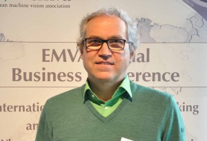
NexWafe also announced that as it meets these important milestones, Peter Pauli will step down as Chairman of the Board of Directors to devote more time to other commitments. He will continue his association with NexWafe and remains a shareholder. "Helping to lead NexWafe on its transition from an academic spin-off to its emergence as a technology product company was a great honor,” Mr. Pauli said. “NexWafe’s EpiNex™ wafers are a key element of the future solar market, as the industry strives to meet expectations in terms of costs and PV efficiency."
NexWafe uses in-line epitaxy for production of high-efficiency monocrystalline silicon wafers. By minimizing waste through its direct-gas-to-wafer manufacturing, NexWafe’s Epinex wafers are fully compatible with conventional solar cell and module manufacturing with a 70 percent reduction in carbon footprint of conventional wafers and at greatly reduced production cost. Using a proprietary process, a crystalline silicon layer is deposited on a seed wafer and then detached, producing finished wafers with an optimal thinness and superior material properties. The company has a 5MW pilot production facility in Freiburg/Germany, with qualification shipments planned to start in 2021 and plans to raise further capital to support that activity. NexWafe was spun out from Fraunhofer Institute for Solar Energy Systems ISE in 2015.