Nanoimprint lithography (NIL) is a high-resolution patterning technique used to replicate nanoscale and microscale surface structures. Unlike traditional optical lithography, which relies on light projection and is limited by diffraction, NIL is a mechanical replication process.
In NIL, a stamp or mold (called a master template) containing nanoscale features is physically pressed into a thin layer epoxy on a substrate. The epoxy is then optically cured (UV Light) to solidify the pattern. Once the stamp is removed, the nanoscale features are left in the epoxy.
Nanoimprint lithography (NIL) has become one of the most promising techniques for fabricating nano- and micro structured surfaces with high precision and low cost. Two main approaches dominate the field today: wafer-scale NIL and Roll-to-Plate (R2P) NIL. While wafer-scale NIL has long been used in semiconductor and photonic device manufacturing, R2P NIL is now emerging as the scalable solution for large-area consumer and industrial applications.
This article compares the two approaches, showing where each excels, how they complement each other, and provides case studies from real-world applications.
Side-by-Side Comparison
|
Feature |
Wafer-Scale NIL |
Roll-to-Plate (R2P) NIL |
|
Typical Substrate Size |
Up to 200–300 mm wafers |
GEN-5 panels (1100 × 1300 mm²) and larger |
|
Resolution |
40 nm – 500 µm |
250 nm – 500 µm |
|
Overlay Accuracy |
High (suitable for multi-layer alignment) |
Lower; suitable mainly for single-layer or tiled products |
|
Throughput |
Moderate, limited to wafer scale |
High; one cycle can produce 5–20× more products via tiling |
|
Cycle Time |
Several minutes per imprint |
<2 minutes per imprint |
|
Stamp Durability |
Hard templates; wear over time |
Flexible stamps; >500 imprint cycles |
|
Material Flexibility |
Mainly rigid wafers (Si, glass, GaAs, InP, SiC) |
Rigid (glass) |
|
Cost per Area |
Medium (precision-driven) |
Low (scaling advantage) |
|
Best-Suited Applications |
Semiconductor memory & logic, co-packaged optics, photonic ICs, biosensors, advanced photonics |
AR/VR waveguides, micro-optics, 3D displays, LiDAR, solar light-management films, functional coatings |
Wafer-Scale NIL: Precision for Semiconductor and Photonic Devices
Wafer-scale NIL is designed for applications where nanometer-level resolution and overlay precision are critical. Its strength lies in high-value industries like semiconductors and photonics, where device performance depends on precise alignment and sub-250 nm feature control.
Key applications:
- Semiconductor memory and selective logic layers
- Photonic integrated circuits and co-packaged optics
- Biosensors and nanopore arrays
- Advanced micro-optics requiring extreme accuracy
Case Studies:
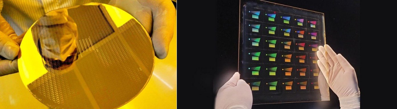
- Biotechnology – Wafer-scale NIL enables replication of nanopore arrays, plasmonic gratings, and SERS substrates on glass or silicon wafers. Wafer-level processing makes it feasible to produce disposable biosensor chips at scale.
- On-chip gratings and Micro-Lens-Arrays (MLAs) – NIL on 200 mm wafers enables cost-effective replication of grating couplers and waveguide elements for silicon photonics directly on integrated circuits and emitters like VCSELs and micro-LEDs.
- Imaging and Sensing - Wafer NIL is used to make microlens arrays directly on CMOS image sensors (CIS). This improves light collection efficiency in smartphones and automotive cameras. Wafer-scale NIL enables integration with existing semiconductor workflows.
- Diffractive Optical Elements – NIL has been utilized to create structured light generators for time-of-flight modules in facial recognition applications.
Roll-to-Plate NIL: Scaling to Consumer and Industrial Markets
Roll-to-Plate NIL addresses the need for large-area replication at low cost. With equipment capable of imprinting panels over a square meter, R2P enables high-volume production for applications where throughput and cost per unit dominate.
Key applications:
- AR/VR displays and waveguides
- Brightness-enhancement and anti-glare films for consumer electronics
- LiDAR and sensing optics
- Solar and energy-harvesting films
- Micro-lenses for advanced 3D displays
Case Studies:
- Augmented reality waveguides – Using R2P equipment, manufacturers have scaled AR waveguide production from single 4-inch masters to hundreds of units per imprint on GEN-5 glass panels, bringing AR glasses closer to affordable consumer products.
- Light-management layers for solar cells – R2P NIL has been applied to perovskite and thin-film solar modules, imprinting anti-reflective textures across large sheets to boost efficiency while lowering manufacturing costs.
Complementary Roles in Industry
Wafer-scale NIL and R2P NIL are not competitors but complements.
- Wafer-scale NIL remains the gold standard for semiconductor-grade accuracy.
- R2P NIL makes large-area consumer products commercially viable.
Together, they expand NIL from the cleanroom to mass-market production, enabling everything from high-performance chips to affordable AR glasses and solar modules.
Conclusion
Nanoimprint lithography is no longer a single technology, but a family of platforms tuned for different needs. Wafer-scale NIL ensures precision at the semiconductor level, while Roll-to-Plate NIL provides scalability and cost efficiency for large-area markets. Case studies show how both technologies are already transforming industries, from advanced memory devices to AR glasses and solar energy. Their coexistence ensures that NIL will continue bridging the gap between advanced research and real-world consumer adoption.
Suleyman Turgut is Head of Partnerships and Innovations at Moveon Technologies.