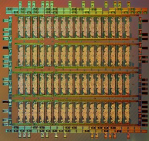
Researchers from the Massachusetts Institute of Technology (MIT), the University of California at Berkeley and Boston University have developed a technique for integrating optical components into existing chip designs. The pioneering system-on-a-chip (SOC) approach, which requires only existing manufacturing processes, would allow adding optical communication components to existing chips with little modification of their designs.
In late 2015, the same team of scientists collaborated on building a microprocessor that integrated electronic and optical components on the same chip using only existing manufacturing processes. The caveat: The chip’s electrical components needed to be built from the same layer of silicon as its optical components, which meant relying on an older chip technology with silicon layers for the electronics that were also thick enough for the optics.
Now, their paper “Integrating photonics with silicon nanoelectronics for the next generation of systems on a chip,” published in Nature, reports another breakthrough:
Assembling on-chip optics and electronics separately
While on-chip optical components are typically integrated into silicon-on-insulator (SOI) wafers, this is not very common for microelectronics. So the team added steps to the microelectronics building process that enabled them to implement optical components without using this type of wafer. “In our approach, we create silicon oxide (glass) islands and then deposit a layer of polysilicon that we use for all of the optical components,” explains Amir Atabaki, research scientist at the MIT Research Laboratory of Electronics and a co-author of the paper. “It takes some effort to optimize this polysilicon layer to have both good optical and electrical properties for the type of high-speed optoelectronic functions that we need on the chip,” he notes. “Simultaneously, we have to make sure that by introducing these additional processing steps we do not touch the performance of the transistors that we need for the high-performance electronics on the chip.”
The new way integrating photonics with silicon nanoelectronics could help to catalyze the development of advanced systems on a chip, the researcher agrees: “Optics can complement electronics in different ways, and our technique can enable necessary optical functions on electronic chips, where needed.”
Solving the communications bottleneck: Adding high-speed optical interconnects to high-performance chips
Atabaki refers to high-speed communication as one of the most important applications of optics. The Internet is based on fiber optic systems. And one of the bottlenecks in high-performance computing today is moving data between microprocessors or between a microprocessor and a memory chip. “Chip manufacturers such as Intel and Nvidia can now use our technique to add high-speed optical interconnects to their high-performance chips to solve this communications bottleneck,” he says.
Using only existing manufacturing processes
One important aspect of this new technique for integrating optical components into existing chip designs is that it requires only existing manufacturing processes. Atabaki argues, for example, that electronic devices are cheap, compared with optical devices, because they leverage economies of scale and learning curves in device manufacturing. “We are offering a technique to build optical devices on these low-cost manufacturing platforms,” he points out. The positively paradigm-shifting consequences? “Firstly, we can manufacture low-cost optical or optoelectronic devices,” says Atabaki. “And secondly, all of the electronic chip manufacturers can add optical functionality without changing their manufacturing process.” The technique could allow the making of chips with a remarkable performance boost from the optics without significant increase in cost.
Building the next generation of systems on a chip
“I would love to see companies that build high-performance GPUs, CPUs and memory chips to use our technique to add optical interconnects to their chips,” says Atabaki on how his team’s research success could effect the design of advanced light-based technologies. “This will allow future computing systems to use optically interconnected chips with at least an order of magnitude higher interconnectivity bandwidth,” he projects. “This can dramatically improve computing power, which could have a huge impact for AI.”
The path and timeline to real-world chip manufacturing
While Atabaki is persuaded that he and his colleagues have “significantly paved the way” for adoption of this new technique, he also points out that, though, it is yet to be shown that the approach can be applied to state-of-the-art nanoelectronics, such as the 10-nm transistor technology used in advanced chips today. “I believe that we have shown very promising results to convince the government or the semiconductor industry to invest the resources to make this happen,” he says, nevertheless. “Our next step is to show that we can use our technique to add optics next to the most advanced transistors, for example today’s 10-nm and the emerging 7-nm technologies.”
Written by Sandra Henderson, Research Editor, Light Technologies Today








 Back to Features