Ocean Insight teamed with leading a supplier of semiconductor solutions to improve processes and product quality in support of emerging electronics technologies such as 5G and the Internet of Things.
Application challenges
Semiconductor device fabrication is a sophisticated process that requires precision in every facet of manufacturing. Maintaining product quality and minimizing wafer loss requires contaminant-free gases and accurate gas mixtures, endpoint detection for plasma cleaning of chambers, and precisely timed deposition and etching endpoint detection.
Traditional methods of monitoring semiconductor chamber cleaning, deposition and etching processes have led to lower wafer yields and chamber degradation. Now, manufacturers can utilize optical emission spectroscopy (OES) and advanced data-processing algorithms for precise, high speed monitoring of processes, resulting in higher quality semiconductor materials for demanding new uses in electronics and nanotechnology.
Spectral insight
In semiconductor processing, trial-and-error methods once dictated chamber cleaning, deposition rates and etching times -- an inexact approach resulting in lower wafer yields, chamber degradation, and wasted resources (Figure 1).

Figure 1. Precise control of chip manufacturing processes results in higher yield and less waste.
Even with technical advances including the use of monochromators to monitor optical endpoint processes, limitations remained. For example, monochromators are limited to single-wavelength analysis, can be affected by optical interference, and are not easily switched out for different production recipes.
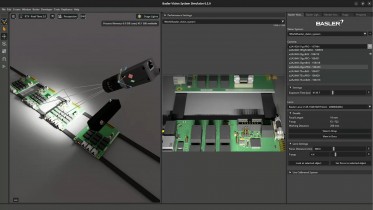
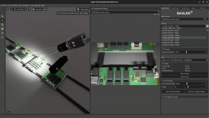
The introduction of optical endpoint sensing measurements using high-speed, precision spectrometers from Ocean Insight has helped to mitigate the limitations of older technologies. With OES, users can quickly and accurately monitor all plasma wavelengths at once, eliminating guesswork. Applying sophisticated algorithms to interpret the measurement data can add another level of insight to process control.
Spectral solutions
GlobalFoundries (GF) provides design, development and fabrication services to leading semiconductor innovators worldwide. Ocean Insight worked closely with GF to address issues associated with an important reactive ion etching process. Managing this “timed etching” process, which was used to determine how long a wafer is exposed to corrosive production gases, relied on a combination of a single-wavelength instrument, knowledge of the variable speed of the chemical reactions involved, and simple trial and error. This often led to over- and under-etching of the product, wasting costly resources.
GF has evaluated the use of modular spectrometers for its systems and will consider rewriting its algorithms to monitor multiple plasma emission spectra to halt etching precisely. The potential impact could be substantial. For example, a single engineer may be responsible for more than 100 chambers, with etch runs that last from 5-25 minutes each. Even small improvements in the etching process could streamline production and improve product quality dramatically.
With Ocean Insight hardware and support, semiconductor equipment suppliers continue to improve and refine the technologies they offer to the semiconductor industry. Their innovation in endpoint detection, plasma-processing and advanced packaging solutions supports emerging technologies related to telecommunications advances, wireless devices, photonics, solid state lighting and MEMS devices.
Written by Rob Morris, Knowledge Manager, Ocean Insight