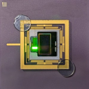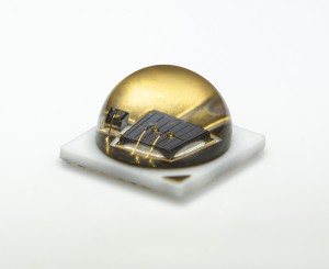
Researchers at the University of California, Davis (UC Davis) in the US have developed speedy silicon photodiodes that could prove to be the missing ingredient to silicon photonics systems and drive down the cost of optical computer-to-computer communications.
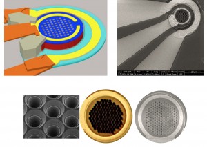
“We came up with a technology that bends the vertically incident light into laterally propagating light in the silicon photodiodes,” says M Saif Islam, professor of electrical and computer engineering at UC Davis. His team achieved this feat by integrating periodic micro- and nanoholes on the silicon surface. “Such lateral propagation of light improves the efficiency of a photodiode, while preserving the speed of the photodiode by keeping the silicon layer thin.”
The professor explains that for a conventional surface-illuminated pin photodiode, speed and quantum efficiency are often a trade-off. To capture most of the incoming photons, the piece of silicon needs to be thick, which makes it relatively slow. Making silicon thinner, on the other hand, makes it work faster, but the photodiode would be a lot less efficient. “Our technology made it possible for a pin silicon photodiode to achieve both high quantum efficiency and high speed at the same time,” Islam says.
Fulfilling the speed demand of optical links at data centers
The rise of the cloud storage and computing has created tremendous demand on data centers to transfer a huge amount of data at a faster speed and lower cost. The silicon photodiode developed at UC Davis can convert data from optical signals to electronic signals at a speed of 20 gigabytes per second, with an efficiency of more than 60% — the fastest yet reported for a device of this efficiency, according to Islam. “This innovation, with its outstanding speed and efficiency performance, and its ability to monolithically integrate with CMOS technology, has the potential to fulfill the demand of the data center optical links component,” the professor says.
Promising both speed and efficiency at potentially lower costs, the research breakthrough could help to finally advance silicon photonics. How? Traditionally, high-speed, high-efficiency photodetectors are made with expensive III-V materials, such as gallium arsenide and indium phosphide. However, as Islam notes, gallium arsenide, for example, is about ten times as efficient as a silicon at the same scale and wavelength. But it is significantly more expensive and unable to monolithically integrate with silicon electronics. “Our innovation has enabled silicon to offer performance that it cannot usually do, and with the benefit of the CMOS integration, the cost of receiver design gets drastically reduced.”
Performance goals for the silicon photodiode
The UC Davis researchers have demonstrated a photodiode operating at 20 gigabytes per second, with a quantum efficiency of more than 50% at 850 nm wavelength, which is commonly used for short-reach fiberoptic links in data centers. Recently, they have even fabricated photodiodes with more than 65% efficiency. Islam reveals they are working on device designs that can provide operational speeds of 60 gigabytes per second or higher — well above the 25 gigabytes per second currently available. The team is also working on integrating these silicon photodiodes with necessary electronics on one single chip, which can drive down the cost of optical data connections.
“Our new silicon photodiodes proved that silicon can be faster than what people anticipated, and, thus, all-silicon optical transceivers can be designed and realized on a single chip,” says the expert, who projects that reducing the cost of connections could push the adoption of optical links beyond data centers. What is more, monolithic integration also enables designs that can be much more power-efficient.
Solving the surface problem
Charge carriers becoming trapped on a semiconductor’s surface is one of the biggest challenges to be overcome in developing this kind of nanostructured photodiode. Why? In the case of the research work at hand at UC David, introducing nanoholes into the device dramatically increases the area of silicon surface, due to the sidewalls of the holes. “Surface of a semiconductor is always problematic because surface is the place where perfect crystalline structure ends abruptly, so it usually has dangling bonds which are electrically active,” explains Islam, elaborating that such places become traps for the charge carriers generated by photons in the photodiode. And trapped carriers cannot reach the electrodes and cannot contribute to the photocurrent. So a photodiode’s efficiency goes down if the device has a large surface area. “This is the main challenge when nanostructures are integrated in photodiodes,” says Islam, whose team has tested many methods and developed processes to make these dangling bonds passive. “One of the most efficient techniques we developed was terminating such bonds with hydrogen,” he shares. “It successfully helped us to eliminate losing our photo-generated carriers and helped our photodiodes to reach high efficiencies.”
Next step
Islam believes the silicon photodiodes he and his team have developed can provide many opportunities in the future. “The next step is to package our photodiodes with some necessary circuitry and test their performance at a system level,” the professor projects. We are also working on implementing similar method to other materials that can grow on silicon wafer such as silicon germanium alloys and germanium. Such material systems are helping us to fabricate ultra-fast photodiodes that can operate at longer wavelengths, such as 1550 nm, which is used for long-reach optical links.”
The paper “Photon-trapping microstructures enable high-speed high-efficiency silicon photodiodes,” co-authored by Islam, is published in Nature Photonics.
Written by Sandra Henderson, Research Editor, Novus Light Technologies Today












 Back to Features