An international team of researchers has for the first time used femtosecond lasers to structurally manipulate bulk silicon. The breakthrough could pave the way to 3D laser writing that would advance silicon photonics applications and could foster a better understanding of new physics in semiconductors.
While femtosecond lasers had long been used to write into bulk materials with wide band gaps, scientists had previously never accomplished precise ultrafast laser writing in narrow-band-gap materials, such as silicon. Even at maximum pulse intensity, femtosecond lasers were not capable of structurally manipulating the bulk silicon.
“For years, scientists from different laboratories in the world have faced one major difficulty in inducing permanent modifications inside crystalline silicon with ultrashort laser pulses, meaning below 100 femtoseconds,” says Margaux Chanal from Aix-Marseille University, France. “We demonstrated that there is no physical limitation to silicon damage inside the volume but only constraints due to the material that can be bypassed.”
Overcoming the limiting factors
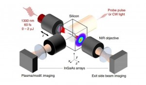
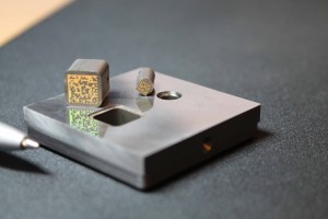
Chanal reports that they were able to understand and identify the reasons why their forerunners were not able to induce permanent changes inside silicon by combining experiments and numerical calculations in the framework of a collaboration between the MINOS Lab and the LP3 Laboratory in France and IESL-FORTH in Greece. “We identified the refraction at the silicon surface — due to the high index of silicon in the infrared (n = 3.5) — as a strong limiting factor to concentrate the light inside the material,” Chanal says. “We had the original idea to replace our cube of silicon by a sphere of silicon, suppressing then the refraction at the surface. The interaction is so intense at the center of the sphere that with very low energy permanent modification has been observed for the first time in our regime.”
Impact on future light-based technologies
The expert agrees that her team’s potentially paradigm-shifting research advance could indeed have significant influence on the development of future light-based technologies. “The main impact is in the micro-electronic field,” Chanal says, adding, “Silicon photonics represents a significative revolution in the micro-electronic field, and 3D laser writing of silicon is a technological progress towards this research domain.”
Breaking through limits
Speaking about what surprised her the most about the outcome of the study, Chanal says, “We had to face a new issue: We needed to concentrate the light more efficiently inside the silicon, but we were limited by the refractive index of our material. The idea of irradiating a sphere inside silicon was totally new in the laser damage field and seemed ambitious for questions of positioning, imaging or characterization of the center of the sphere.” The researcher goes on to note that on top of that each attempt to modify the silicon consumes one sphere, since they damaged the center in the process, and the target needs to be changed every time. “The most surprising thing was that our numerical model predicted that with a focusing objective with a numerical aperture of 0.85, the center of the sphere will be damaged,” she says. Until then, they had not succeeded when they tried a smaller numerical aperture. But, as predicted, the aperture of 0.85 ultimately lead to the breakthrough result, with very low energy of 5 nJ.
The next step
Chanal projects that this study has two potential future applications: “From a fundamental point of view, the high confinement of this new interaction inside a sphere induced millibar pressures, and we aim to discover new phases and new materials,” she says. “From an industrial point of view, we are now thinking of adapting our process to the industry of silicon photonics.”
The research is described in the paper "Crossing the threshold of ultrafast laser writing in bulk silicon,” published in Nature Communications.
Written by Sandra Henderson, research editor Novus Light Technologies Today









 Back to Features