


German high-tech company AMO provides research and fabrication services in the field of nanotechnology. Michael Hornung, Managing Director, sat down with EPIC’s Jose Pozo to discuss driving research and process development in the areas of graphene electronics, nanophotonics, nanoimprint, and sensor technology.
Michael’s early career was launched after he graduated in 1992 with an MSc in Mineralogy from the University of Freiburg in Breisgau, Germany. Having developed a fascination for crystallography, he then pursued a PhD focused on the growth of crystals in copper-indium-selenium systems and on the characterization of their microstructure. After receiving his doctorate in 1996, Michael remained in Freiburg, spending the next 4 years as a Research Scientist, working on the construction of detectors based on gallium arsenide for the Large Hadron Collider (LHC) at CERN, in Geneva.

The interest on gallium-arsenide based detectors was motivated by the expectation that, being this material radiation hard (unlike silicon), it would be able to withstand the enormously high levels of radiation created inside the collider. Unfortunately, tests proved this not to be the case, and the project was ultimately abandoned. Michael then spent the rest of his post-doc time developing readout electronics for CERN.
SUSS MicroTec
In 2000, Michael’s postdoc contract came to an end. Although working at CERN had been a great experience – collaborating with scientists from all over the world and meeting several Nobel-prize winners including Stephen Hawking – Michael knew that with his background in mineralogy it would have been difficult to continue working in high energy physics. Accordingly, he successfully applied for the post of Application Engineer at SUSS MicroTec in Germany.
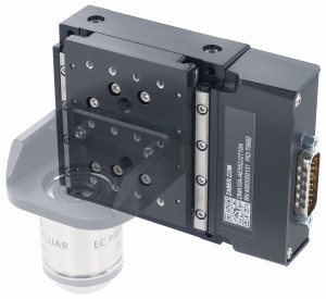
SUSS MicroTec was, and still is, a leading supplier of equipment and process solutions for microstructuring applications, including backend lithography, wafer bonding and photomask processing, as well as micro-optical components. Michael’s first task at SUSS Micro Tec was to equip a clean room with all the tools required for lithography, and to demonstrate the company’s various lithography processes to potential customers, in relation, for example, to etching, mask aligning, coating and different substrate materials.
In 2006, Michael became Application Development Project Manager, and was responsible for finding ways to improve lithographic nano-imprinting processes. In this context, he successfully introduced the first imprint resist using a UV curing glue. But the real breakthrough came when his team implemented Philips’ SCIL (Substrate Conformal Imprint Lithography) technology, which for the first time, enabled high quality and high-resolution nano imprinting.
In 2011, after receiving an MBA from at Ludwigshafen University of Applied Sciences, Michael was promoted to one of SUSS’s Technical Marketing Manager, becoming responsible for nanoimprint lithography, LED applications and leading research projects with research institutes, universities and other companies to achieve company targets.
AMO GmbH
Towards the end of Michael’s time at SUSS, there was a change in management. If before he enjoyed a certain level of independence, with the new management regime he had to pass everything through his boss and to fight for every decision. Unhappy with the situation, in 2014, Michael decided to move to AMO GmbH as Chief Operating Officer.
Based in Aachen, AMO is a research foundry and a non-profit nanotechnology SME, which follows the mission of closing the gap between university research and industrial application. AMO acts as a scout for new technologies, identifying topics from basic research that looks particularly promising for future applications and developing their potential towards industrial manufacturing. It also provides research and fabrication services, from proof-of-concept demonstrators to final technological solutions, building on its broad expertize on advanced nanolithography techniques (UV- Nanoimprint, E-Beam lithography, Interference Lithography) and on a highly flexible CMOS-environment.
What drove Michael to AMO was the possibility of getting back to the world of cutting-edge research, and of having more control over decision-making. Shortly after arriving at AMO, Michael became one of the two CEOs, and he has since been responsible for driving research and process development in AMO’s four areas of expertise.
Graphene electronics. Hundred times stronger than steel, incredibly flexible, and completely transparent, graphene is an exceptional material, with a huge spectrum of potential applications, including anti-corrosion coatings and paints, efficient and precise sensors, faster and efficient electronics, flexible displays, efficient solar panels, faster DNA sequencing and drug delivery.
AMO is exploring the potential of graphene in micro- and optoelectronics since 2006. But, as Michael emphasises, being a bridge between basic research and industry, AMO’s role is not just to engage in research but also to show how particular processes can be scaled up for mass production.
To this end, AMO has teamed up with other key European companies and research centres to create the 2D-Experimental Pilot Line, a first-of-its-kind manufacturing facility for graphene and 2D materials. Funded under the EU’s Horizon 2020 program, the aim of this pilot line is to demonstrate how electronics, optoelectronics and sensors based on graphene and other 2D materials can be produced for commercial applications.
Nanophotonics. When AMO was founded in 1993, the focus was mainly on silicon technology for classical CMOS processors. Since then, AMO has also developed a core competence in employing state-of-the-art clean room structuring technologies to develop active and passive integrated nanophotonic structures and devices, such as high-speed integrated modulators and resonators for modern optical communication applications.
More recently, AMO has also set up a second nanophotonic platform using silicon nitride as waveguide material for applications in information technologies, bio-photonics, life sciences, sensing, and integrated silicon-based components for terahertz generation.
Nanoimprint: Since feasibility and costs are the decisive factors for the development of successful nanofabrication techniques, AMO keeps investigating the most suitable low-cost replication technology for e-beam defined nanopatterns, by combining the advantages of low imprint-force and precise alignment capabilities to obtain a resolution limited only by the template. An important result has been the development of high performance a UV-curable resist (AMONIL) and a matching adhesion promoter (AMOPRIME), which are now commercially available.
AMO is also involved in several national and EU R&D projects to explore the potential of replacing expensive EUV lithography for industrial applications in photonics, NEMS and biotechnology.
Sensor technology Using the accumulated know-how in material processing and advanced replication technologies, AMO is working on sensor technology for applications in safety engineering, biotechnology, pharmaceutics and environmental technology – e.g. for detecting medical residues and other hazardous materials in waste water.
Since the core of sensor technology is the ability of transforming one type of energy into another one that can be handled more efficiently, AMO also invests this expertize into environmental and energy related projects. For example, AMO is currently participating in HyperSol, an EU funded project to explore plasmonically-enhanced photocatalysts’ to increase the production efficiency of solar fuels.
The future
In 2021, AMO has started a dozen of new R&D projects, mainly funded by the EU’s Horizon 2020 program. These include projects on the development of graphene-based, ultra-fast photodetectors; on the development of ultra-compact, low-cost plasmo-photonic platforms for food quality monitoring; and on the development of novel optoelectronic components based on 2D materials and perovskite semiconductors.
Furthermore, AMO is also exploiting its technological platform and know-how in emerging fields such as quantum computing and artificial intelligence. In this context, AMO is contributing to the EU-project MISEL, which aims at developing a multispectral intelligent vision system with embedded low-power neural computing. Other two ongoing projects related to AI are: AI-NET-PROTECT, which aims to use AI to provide automated resilience and secure networks against cyber-attacks, and AEOLUS, which target a cloud-connected system for monitoring air quality based on highly integrated mid-IR photonics and powered by deep learning algorithms. Furthermore, AMO is involved into the projects Neurotec and NeuroSys, two major initiative funded by the BMBF for developing the technological basis for neuromorphic devices for artificial intelligence applications.
As Michael points out, these are all areas where future progress will most probably rely on the successful integration of new materials into classical semiconductor manufacturing lines based on silicon. This type of integration is, since years, one of AMO’s strengths, and it will keep playing an increasingly important role for future projects. Another reason why companies and research institutions will keep seeking AMO’s collaboration is because they know that having shown that a device works, AMO will try to improve the technology and make it ready for manufacturing.
If you started again, what would you do differently?
“To be honest, not much. I haven’t had many failures and when I look back at my career, I think I mostly made the right decision at the right time. I suppose I could have left SUSS earlier, but then again, the experience and know-how I accumulated with them has been invaluable”.
What advice do you have for the next generation of entrepreneurs?
“First, it’s important to be open to foreign cultures and different views of life. Don’t just work on your own with your own ideas, look over the border and see what’s happening in other places and what is coming from other directions.
Second, you need to be opened to change. The worst thing you can do is to remain stuck on the same path and not be aware of or refuse to implement new processes or new technologies.”
Written by Jose Pozo, Chief Technology Officer at EPIC (European Photonics Industry Consortium).