


KNT (Kelvin Nanotechnology) is an internationally recognized provider of advanced photonics and quantum components, and is a photonic fabrication service provider for diverse market sectors. As one of the first suppliers of miniaturised quantum components in the market, KNT produces 3D ion traps, grating MOTs, MEMS gravimeters and specialist DFB lasers for international partners and customers. They are driving forward innovation in fabrication of quantum components to support quantum systems for information processing and computing, chip scale cold atom systems, sensors and high precision timing and navigation.
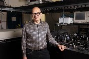
Jose Pozo, EPIC’s CTO, had the opportunity to talk to Brendan Casey, CEO of Kelvin Nanotechnology about his early research at the University of Glasgow and the formation of the subsidiary company, Kelvin Nanotechnology.
In 1994, in his final year of a BSc in Electronics Engineering at the University of Glasgow, Brendan worked in a clean room making devices for DNA sequencing. It was a side of electronics he had not been unaware of before, and he found the work fascinating. He was fortunate to work under the supervision of Professor Chris Wilkinson, a real expert and trailblazer in fabrication who introduced Brendan to the bio side of the technology.

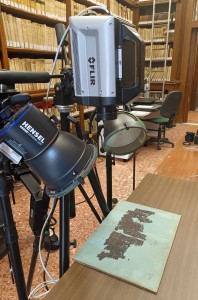
Accordingly, upon graduating, he embarked on a PhD in Bioelectronics. With a lifelong passion for making things, his research was very hands-on: fabricating artificial environments for DNA sequencing, devices for cell testing and implants for things like tendon regrowth. During this period, Brendan became an expert in electron beam (e-beam) lithography and worked with both tools and software to push the limits of what was possible with the technology. Electron-beam lithography involves scanning a focused beam of electrons to draw custom shapes with sub-10 nm resolution onto a substrate. The aim is to create very small structures that can then be transferred to the substrate material by etching or depositing metals, insulators, biocompatible materials, optical or electronic layers. Applications include devices such as laser gratings, transistor gates, imprint masks, optical elements, photonic crystals, nanotextured surfaces for the photonics, quantum, and telecoms industries.
After his PhD in 1997, he worked as a Postdoc Research Assistant at the University of Glasgow focussing on the use of e-beam lithography and nano-imprint lithography for optical devices. His original aim had been to go into academia, but he found the work so enjoyable that in 2000, he decided to forego academia and accept a job as Electron Beam Lithography Senior Engineer with Kelvin Nanotechnology Ltd (KNT) a newly created subsidiary company of the University of Glasgow.
Kelvin Nanotechnology
During the 90’s, the University of Glasgow began to gain an international reputation as a fabrication expert in the field of electron beam (e-beam) lithography and nanofabrication. By 1997, they were receiving so many International enquires for rapid prototyping that they decided to create a subsidiary company of the university, Kelvin Nanotechnology Ltd. (KNT), which would enable a 100% focus on commercialising the technology without teaching or any other academic constraints.
Company development
Shortly after he joined KNT, the company received a large wafer production order, which paved the way for a move away from pure R & D to small volume production. Then, following the telecom crash in the early 2000s, they began to pivot into different sectors based on a strong underlying need for photonic devices, and in 2003, Brendan was appointed NKT’s Business Manager.
The next landmark was in 2006, when the James Watt Nanofabrication Centre opened at the University of Glasgow and when KNT was funded as part of the UK’s micro nanotechnology network. This allowed KNT to offer a real commercial service based on quality and timely delivery and over the next three years the company’s workforce grew from 2 to 9 employees.
In 2011, with KNT doing well and having acquired an international reputation in the e-beam lithography and nanofabrication market, Brendan was offered the position of CEO to lead the company through its next stage of development.
Since then, the company has developed in two main areas. First, using the increased fabrication capability provided by the new James Watt Nanofabrication Centre, KNT has initiated a number of innovate projects with partners as part of a consortium to develop new technologies particularly in quantum. This has proved very fruitful and made a significant difference to the company’s growth and technical capability. The second strand of the strategy has been to build a highly competent technical team by recruiting the best people available and fostering an environment of training and development.
Current technology
Brendan has developed a two-pronged strategy for developing KNT’s technology. Firstly, rather than offering a broad range of products for a narrow market, the company offers a narrow range of products and services for a broad range of markets. Secondly, in order to provide flexibility and stability in the face of market vagrancies, KNT offers services in three main areas, as follows:
1. High resolution, large area, multi-level electron beam lithography for photonics, quantum technologies and telecoms industries. Applications include devices such as laser gratings, transistor gates and imprint masks. In this field, KNT’s experience and expertise enable them to get jobs done quickly and cost effectively.
2. A wide range of proof of concept, feasibility, and prototyping services for the semiconductor, optoelectronic, bioelectronic and nanoelectronic markets.
3. Quantum Components: Since 2015, KNT has become a globally recognised supplier of quantum devices and components. Their current portfolio of components includes
Magneto Optical Trap Gratings (gMOTS): Originally published in ‘Nature Nanotechnology’, gMOTS are diffractive optical elements that improve ease of alignment, setup and miniaturisation for cold atom source creation compared to conventional 6-beam MOTs. Cold atoms formed in these traps are a key component of quantum-based technologies e.g., for applications for precision timing and sensing for space and global navigation systems, and timing for financial trading systems and data networks.
Micro Ion Traps: Originally published in ‘Nature Nanotechnology’, these 3D micromachined ion traps, using a wafer-scale process co-developed with NPL and Alter, enable the trapping of multiple ions. The microfabrication process ensures reproducibility of device dimensions, scalable manufacture and makes them an excellent platform for an elementary component in quantum devices such as clocks, sensors, and quantum computers.

Wee-g portable gravimeter: First published in ‘Nature’, this MEMS technology enables a reference, low power, no need for calibration, deployable and highly sensitive device. It can be used to measure small variations in density underground to create gravity images required, for example, for energy, civil engineering, defence, and environmental monitoring.
The future
Brendan’s preferred future over the next five years, is for the company to begin to scale manufacturing of quantum-based photonics devices to enable deployment of miniature, portable and cost-effective systems. This would be both a paradigm shift in quantum technology and also the culmination of a journey for KNT from theoretical publications in Nature to the actual production of devices for next generation quantum computing, quantum enabled navigation systems and quantum sensors.
In this context, he believes strongly that Europe and the UK need to develop a strong quantum manufacturing capability. As he is keen to emphasise, it’s not just a matter of ensuring wealth and job creation; more importantly, it will help to diversify the sector beyond PhD researchers to a much broader part of the community – hopefully, to the extent that quantum technologies become an aspirational career choice for young people at school, as an alternative, for example, to financial services.
If you started again, what would you do differently?
“Looking back at my early career, I think today, I’d be less risk-averse. I’ve come to realise that in the early stages, you have much more flexibility than you think, and you can sometimes underplay your worth and capabilities. That’s why I try and work with our younger employees to empower them to take risks and to trust their instincts. I would say this is something that's true in all stages of your career. Afterall, providing you recognize you’ve made a mistake quickly, making a mistake is not fatal; if you get something wrong, you're just in a different location and you can easily and quickly adjust and change course”.
What are your words of wisdom for the next generation of entrepreneurs?
“First, there’s a tendency for young entrepreneurs to feel under pressure to know and understand all aspects of their business, but there’s hardly anyone in this position. For this reason, it’s important to identify areas where you’re not as strong as you need to be and then look for people who can help”.
“Second, in looking for advice, it’s a good idea to identify two or three experienced people you trust who are willing to serve as mentors on a long term basis to help you develop all aspects of your skill set. In my case, when we became part of the micro nanotechnology network in UK, we were advised to set up an industry advisory board. This gave me the opportunity to identify three mentors who were hugely experienced in areas such as operations, marketing and sales, and general business management. Fifteen years later, we still meet regularly, and this has been the most invaluable part of my career development. Not only has it helped me understand the business and make better decisions; equally important, being a CEO can be quite a lonely place and my mentors have been people I’ve been able to confide in and ask for advice without fear of judgement”.
Written by Jose Pozo, Chief Technology Officer at EPIC (European Photonics Industry Consortium).