


Henning Schröder is Group Manager Optical Interconnection Technologies at Fraunhofer IZM Berlin, a group responsible for the development of innovative packages for components and systems for microelectronics, optics and microsystems technology. Ivan Nikitski, EPIC’s Technology Manager for Quantum and PICs, had an opportunity to speak with Henning to learn about is responsibilities and plans for the future.
What’s the background to your appointment as Group Manager of Optical Interconnection Technologies at Fraunhofer IZM Berlin?
In 1988, I went to the Otto-von-Guericke University Magdeburg to do a BSc/MSc in Physics. My studies focused on ultra-high vacuum physics and MEMS technology, and in 1995, I went to the Technical University of Berlin do a PhD. My work was related to micro-optical MEMS, in particular, the development of a mechanism for anisotropic etching of silicon i.e., the removal of material in specific directions to enable the production of geometric characteristics used in MEMS manufacturing.
In 2000, after my PhD, I successfully applied to Fraunhofer IZM, who were also developing MEMS technology and MEMS packaging, and started a very small group dedicated to photonics. I’ve been at Fraunhofer ever since as Group Manager of the Optical Interconnection Technologies working group, and we now have a team of 20, comprising PhD scientists, engineers and technicians and about 15 students.

How has the technology evolved over the past 23 years?
Since it was founded in 1993, the Institute’s main aim has been to take research out of the lab and into industry. In the early 2000s, at the hight of the telecom bubble, we focused on fiber optics and connections for telecom systems and data centers. Since then, we’ve had to follow developments in chip technology with new kinds of electrical and optical interconnects, which have presented new challenges for packaging. We’ve had to step more and more into more precise structuring technology using glass to play between active and passive alignment of the components. An important change took place about 15 years ago when we brought in Ficontec bonding machines so we could move to automization and take photonic integration out of the lab to manufacturing.
Throughout my time at Fraunhofer, my aim has been to transfer the lessons learnt from microelectronics packaging to photonics. In the early days, we were 20-30 years behind microelectronics - in the other departments around me, they were using flip chip, die and wire bonders – all automates. Fortunately, photonics has caught up and, in my lab, we now have the several high precision bonders and other high troughput equipment that we can transfer after process development.
What do you offer to clients and collaborators?
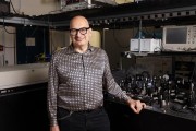
I head an R & D group for photonic packaging and optical interconnection technologies for printed circuit boards and photonic modules. We have all the main technology lines required for this, such as wafer level system integration and printed circuit board technology, which we combine with panel level approaches to get new innovations. Our main area of work is the design, fabrication and performance enhancement of optical glass waveguides and micro-optics for PCB and optical sensors, as well as reliable micro-optical assembling and packaging technologies for photonic modules including optical fiber attachment.
Who are your customers?
We do R&D together with start-ups to large companies, which accounts for around 50% of our business, as well as large European, national, and regional funded projects, which account for the other half.
Our work with start-ups typically involves helping them to integrate chips into their system so they can create a first prototype to show VCs and potential customers.
Medium to large companies usually want to find specific solutions regarding processes and/or materials or for specific chips. Most activities are related to new PICs on different substrates such as silicon-on-isulator, silicon nitrite, and lithium niobate etc. In this area, the work involves structuring substrates, gluing and soldering of contacts, aligning the fibres, and ensuring reliable high coupling efficiency. We also resolve thermal and high frequency issues, and if necessary, in combination with microfluidics.
Larger companies tend to have longer projects that are more strategic and usually involve more money. For example, we help big chip suppliers to integrate their chips into systems, advising on the most appropriate substrate. There are also the application related companies like Siemens and the big automotive companies, who typically who want to shrink an electronic photonic system. For example, we have fiber optical gyroscope projects where customers want to miniaturise and combine the electronics and photonics in a very small form factor.
Then there are communication companies and data center equipment providers, who are looking for power efficiency for smaller systems and need system integration to get more functionality. We are also providing solutions for quantum communication, quantum sensing and quantum computing, where miniaturization and packaging technologies are more and more essential.
A major advantage of working with us is that the Institute is equipped with a range of state-of-the-art reliability test and failure analysis equipment, so we can see exactly how systems beave and fix any problems.
Where do you see future growth?
One trend is the chiplet, a tiny integrated circuit that contains a well-defined subset of functionality. Chiplets are a challenge for packaging, and we are seeing an increasing demand for short range electrical and photonic interconnection of chips that provide high power efficiency and band width. In the pure electronics domain, one growth area is power electronics, which are important for electric cars and renewable energy. Another growth sector is sustainability or green electronics, whereby electronics and photonics are designed at the beginning to be recyclable and power efficient.
What are the future challenges for photonics packaging?
The well-known difficulty is the lack of standards. Those working with PICs are improving their processes every day, but the variety of substrates and lack of standards create cost and scaling problems. One technical solution we are providing is to use selective laser induced etching to structure glass substrates in a precise, flexible and three-dimensional way. In combination with precise laser bonding technologies, this glass-based technology is cost effective and enables a lot of packages for photonic systems. The next step is to move from wafer level to panel level integration. This will allow opportunities to use printed circuit board technology in some way, which is becoming more precise and cleaner, but also trickier for integration on a large panel format.
What will be the main drivers for photonics integration in the future?
For communication applications, it will be more band width and lower power consumption. In the sensing domain we see a continuing trend towards miniaturisation to enable the manufacture of low cost and high-volume applications particularly for IoT, point-of- care equipment, and environmental applications.
At this point, I’d like to announce that on 4-5 June 2024, Fraunhofer IZM are hosting an EPIC Meeting on Photonic Integration and Packaging in Berlin. The aim is to look at advancements in chip-scale integration, advanced packaging techniques, and novel manufacturing processes and how these advances are going to revolutionize various sectors, including telecommunications, data centers, healthcare, and sensing applications. Everybody working on technology in these areas is welcome to attend, as are manufacturing companies who would like to learn more about new trends in materials and components and what’s new from the technology point of view.
I’m aware that many companies are reluctant to move from pure electronics to combined electro-optics and photonics because of the cost and technical problems involved. But this meeting will be a great opportunity to learn how they can benefit from photonics and increase their future competitiveness.
What’s your advice for the next generation of researchers?
I'm a friend of the little things. Young people studying physics today tend only to see old school optics: big lenses and large optics. My advice is to look at butterflies and the small eyes of flies and other animals, and to get inspiration for innovative small products that can drive the future of micro-optics and open up new avenues in physics. But most relevant: try do solve relevant problems to transform our world to a sustainable one.
Written by Ivan Nikitski, EPIC’s Technology Manager for Quantum and PICs.