


At the age of 9, Daniel Schall made his first transistor radio. It worked, so he took it to school to show his classmates. But when he was asked how the transistors worked, he couldn’t answer, so that afternoon, back at his house, he cracked open one of the transistors with a pair of pliers to see what was inside. Unable to detect anything, he investigated further with a hammer and some more tools, but to no effect. He knew the transistor was a kind of switch, but how could it switch something when there were no moving parts inside? And so began his passion for electronics.
His fascination with transistors stayed with him until 2004, when he went to Darmstadt University of Applied Sciences to study an MSc in Microelectronics and Automation. After attending classes on the functions and simulation of transistors, he finally found out how they worked, but then came the question of how a billion transistors could be manufactured - a topic he addressed in his master’s thesis. During his studies, he founded a recording studio for carrying out audio engineering and live mixing, and he also worked freelance for an engineering consultancy designing security and electrical systems mainly for prisons.
After graduating in 2009, he went to RWTH Aachen University to do a PhD in Electrical Engineering and as part of his course, he worked at AMO GmbH, a non-profit, nanotechnology research organisation, where he researched silicon photonics and graphene-based transistors and photonics.

After his PhD in 2016, he stayed on at AMO as a researcher and later group head, working on techniques to improve the energy efficiency and performance of chip technology with the aim of getting it ready to meet the future demand for performance-hungry applications such as AI, communication in data centres, 5G networks, chip-to-chip communication, and optical on-chip sensors.
Central to this research was the knotty problem of how best to combine electronics and photonics. At that time there were two strategies: to bond photonic circuits on electronic chips or to use silicon photonics. However, it became increasingly apparent that the first option would be too costly and not allow scaling, while silicon photonics could not, ultimately, provide the required performance. Most importantly, both approaches would not allow directly mass-producing photonic interfaces on any chip.
Black Semiconductor
It was this search for high-performance, low-cost chips with electronic and photonic functionality that led Daniel and his brother, an economist, to set up Black Semiconductor in January 2020, with Daniel as CEO. As he explains, although multiple chips can be connected, laterally or stacked, at some point the chips need to be connected with optical interconnects as they are too far away from each other to use conventional electronics. This touches the fundamental principle of the scaling strategy of the semiconductor industry: Up until now, higher performance was obtained by increasing the number of transistors per chip by downscaling the transistors. The shrinking gets more and more complicated and expensive, and, eventually, will end. One way to continue increasing the number of transistors in one system is to connect chips to each other. The problem is that very soon the distance between the chips is too large, so that conventional electronic communication would fail.
The paradigm shift that Black Semiconductor is introducing is that it removes the boundaries of each chip by allowing to create fabrics of chips. This upscaling of transistor counts by allowing it to create networks of optically connected chips with fully integrated photonic interfaces it the key to dramatic performance improvements. Black Semiconductor was set up to develop a technology that allows mass production of high-performance photonics on any electronics.
As they had both already set up their own companies, Black Semiconductor was seen as the next phase of their entrepreneurial journey. Based in Aachen, Germany, the company’s mission would be to manufacture and market extremely powerful microchips with integrated electronic-photonic circuits that would represent a paradigm shift in chip technology.
Company development
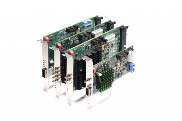
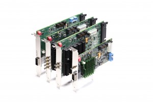
The first step was to convert their ideas into a specific technical product based on a photodetector that Daniel had developed as part of his PhD thesis. With the support of AMO, they then started to write funding proposals, which resulted in them being awarded a grant from the prestigious Exist program, a German federal government funding scheme to help technology and knowledge-based business start-ups. This funding enabled the company to take care of the business side and to further develop the technology. However, the original idea of developing the photodetector was soon abandoned, as although it was a good product, it could only be used for niche applications and was therefore not suitable for high-volume production. Consequently, they changed the concept to where they are today, i.e., not just a photodetector, but the integration of the detector and modulator into an integrated circuit, comprising a transmitter and a receiver with photonic links between the interfaces, so that chips can be connected with fibres or interposers. The advantage of this integrated approach is that it’s far more scalable and wide ranging as it allows mass production of high-performance photonics on any electronics, for example, to enable ultrafast data transfer and photonic signal processing as used in AI systems as well as spectrometers for medical applications.
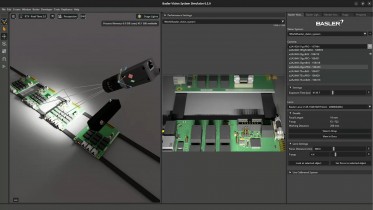
To showcase their technology, Black Semiconductor is currently working on the development of demonstrators, which will involve more R&D, and with a workforce of 13 employees, additional private investment. Although they won’t have a product available in the immediate future, they are discussing their ideas with potential customers - particularly those companies interested in resolving the current bottleneck in data processing, namely, the need for high-speed data exchange and a closer memory.
Challenges
A main challenge continues to be how to effectively communicate their ideas and to get feedback from prospective customers, investors, and employees. Convincing customers of the advantages of a disruptive technology is always difficult, partly because of the inherent conservatism in the industry, but also due to differences in the technical knowledge of the people they must deal with. The easiest to convince are the scientists because although the technology is still difficult to explain, they know enough to ask the right questions. But investors and those with non-technical backgrounds need a different language, and a major challenge is making sure that Black Semiconductor’s own team is aligned in how to communicate and transport the company’s ideas to all its stakeholders.
The future
For Daniel, the future looks bright: they have the technology in place, and they are confident of resolving future engineering issues that will allow them to achieve reproducibility and mass production. Most importantly, they have secured private investment from an excellent consortium among which are Vsquared Ventures, Cambium Capital, and Project A, and most notably Hermann Hauser, the founder of ARM, a British semiconductor and software design company based in Cambridge, and Andy Bechtolsheim, co-founder of Sun Microsystems. The main challenge now is to grow the team while simultaneously keeping communication intact so that everyone is on the same page - something that is difficult when a company is growing quickly.
Key to their future growth and development will be the continued use of the divide-and-conquer approach to problem-solving, also known as decomposition in computer science. With this approach, complex problems are broken down into smaller, easier-to-solve sub-problems, which are solved independently. Sub-problem solutions are then combined to resolve the original larger problem.
If you started again, what would you do differently?
To be honest, not much. I would still pursue the same passions and interests and follow the same path as I have done up to now.
What’s your advice for the next generation of entrepreneurs?
Firstly, be passionate about your technology and look for a mentor in your chosen field so you can fully learn how the technology works and how it can be used in the real world.
Secondly, you only have one life, and the business and private parts are inevitably interrelated. So, to have fun and be happy in your work, it’s necessary to adopt a holistic approach because in the end, everything is connected.
Written by Jérémy Picot-Clémente, EPIC’s Photonics Technologies Program Manager.