New findings by researchers from the University of Potsdam and the Helmholtz-Zentrum Berlin (HZB) could revolutionize the design of perovskite solar cells. Photoluminescence techniques with high precision, spatial and temporal resolution allowed extremely accurate measurements on 1-square-centimeter perovskite cells, which enabled the teams to identify the decisive loss processes in perovskite solar cells that limit the efficiency.
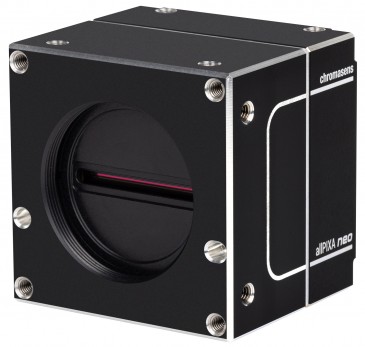
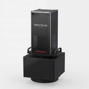
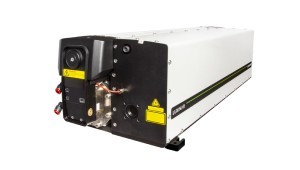
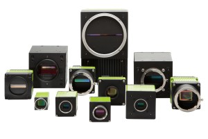
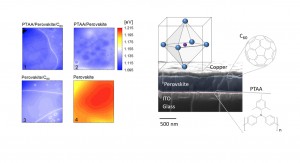
To determine where these defects were located within the perovskite layer — i.e., mainly within the perovskite layer or preferentially at the interface to the transport layer — the researchers excited the perovskite layer with laser light and precisely measured the exact number of emitted photons and recorded and analyzed the photons´ energy using a hyperspectral CCD camera. The method allowed them to calculate the losses at every point of the cell.
The findings
“Using our approach, we are confident that we can pinpoint the source of detrimental non-radiative recombination in perovskite cells,” says Dr Martin Stolterfoht at the University of Potsdam, speaking on behalf of Professor Dr Dieter Neher, who led the study. “Starting from the unoptimized standard cells, we found that the major recombination pathways limiting the cells´ efficiency are located at both perovskite/charge transport layer interfaces at the bottom and at the top.”
The conclusions
“What we clearly see from these studies is that the perovskite material would allow much higher open-circuit voltages than presently achieved, and we conclude that the real challenge to improve this technology to its radiative limit lies in suppression of interfacial recombination at the perovskite/charge transport layer junctions,” says Stolterfoht. “One can estimate that 25% power conversion efficiency will be readily within reach if the selectivity of the transport layers can be further improved, while further perovskite morphology improvements will further accelerate this development and allow even better devices.”
The measurements showed that the “worst” defects are located at the interfaces between the perovskite absorber layer and the charge-transport layers. Thus, adding additional “protective” layers in future cell designs could help to mitigate losses and significantly boost conversion efficiencies. “We hope that future efforts will increasingly aim at reducing the detrimental recombination at the perovskite/charge transport layer junctions by blocking the minority carrier away from the wrong interface,” Stolterfoht says.
In particular, he proposes focusing on the interface to the top electron transporting layer, the fullerene C60 in their studied solar cell architecture, as this material is not perfectly blocking the holes. In the study, the recombination loss current at the perovskite/C60 interface, for example, was roughly 30 times larger than in the whole perovskite bulk.
“As to the perovskite material, we concluded that it does not substantially limit our present cells, simply because the recombination at the interfaces is so much worse,” Stolterfoht says, adding that to really push this technology to its fundamental thermodynamic limits of more than 30% efficiency would require substantially lowering the perovskite defect density further, which could reduce the recombination loss current by more than 10 times. Various metal oxides, non-fullerene organic semiconductors, chemical dopants or other interfacial (blocking) layers could be promising and potentially more suitable electron transport materials.
Extremely precise photoluminescence technique
Photoluminescence is a tool that essentially measures the emission of a device under illumination with a light source. “Essentially, if one knows how many photons are absorbed by the device and how many photons leave the device, one can determine the so-called photoluminescence quantum yield, which is simply the ratio of emitted to absorbed photons,” Stolterfoht explains, adding that standard solar cell theory — by pioneers like Shockley and Queisser — explains how this radiative efficiency is linked to the free energy a cell can produce or, likewise, the maximum efficiency it can achieve. “This theory essentially says that a perfect solar cell must be a perfect LED to achieve maximum performance,” the expert says. “By measuring this emission from every component of the perovskite stack we can in principle determine the limitation from every individual component of the stack. Moreover, for each component we can also look at the spatial distribution of the emission, which essentially allows us to look at defects along the lateral dimensions of the active layer.”
Conversion efficiency improved by well more than 20%
The research work discussed here is based on so-called pin-type perovskite solar cells, where the perovskite is sandwiched between a hole-selective layer at the bottom and an electron-selective layer at the top. This cell architecture is very attractive, according to the researcher, because the devices require only ultrathin transport layers, without high-temperature treatments or chemical doping. Furthermore, the good compatibility of pin-type perovskite cells with well-established p-base silicon cells is advantageous for tandem solar cell applications. Recent advancements have enabled silicon/perovskite tandem cells with efficiencies around 27%.
“The novelty of the cells in this study is based on two additional ultrathin interfacial layers between the perovskite and the above-mentioned charge transport layers, which suppress the identified recombination losses,” Stolterfoht says. “We thereby achieve around 20% certified efficiency for 1 cm2 large cells — currently a record for pin-type cells of that size — and 21.6% efficiency for smaller cells, which is also among the highest reported values.”
Next steps
Stolterfoht and his colleagues are currently extending this approach to a broad range of popular and commonly used charge transport layers for all major types of perovskite solar cells. He says, “And of course we also aim to further improve the device efficiencies through multiple interfacial engineering approaches and perovskite optimizations. We believe there is still a huge potential for further improvements and we hope we can further contribute to the rapid development in this field.”
The results were published in Nature Energy. The paper is titled, “Visualization and suppression of interfacial recombination for high-efficiency large-area pin perovskite solar cells."
Written by Sandra Henderson, research editor Novus Light Technologies Today













 Back to Features