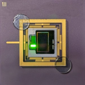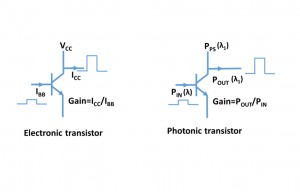
A team at the A*STAR Data Storage Institute (DSI) in Singapore are working on a photonic transistor for optical interconnects that can control light signals. Based on prevalent semiconductor technology (CMOS manufacturing), the new design could be a game-changer for optical signal processing. Advantages include high switching gain, low switching power and high operating speed.
"Our design consists of a circuit of coupled silicon waveguides that guide infrared light with conventional telecom wavelength of circa 1.55 um," says A*STAR DSI scientist Vivek Krishnamurthy. "Some of the waveguides feature an optically active material, such as an indium-gallium-arsenide-based semiconductor, that can amplify or absorb signal light depending on whether or not it is optically excited. During operation, the intensity of a short-wavelength routing beam is used to control the strength of an output beam by altering the amount of absorption and gain in the circuit."
Electronic transistors not only pose a bottleneck for data processing speeds and chip size but a considerable portion of energy is wasted as heat. Replacing electrical interconnects with energy efficient optical interconnects that carry data using light signals could be a game-changer for data processing. "There is no power consuming electrical bias that is required in conventional semiconductor optical amplifier-based all-optical switches," Krishnamurthy explains. The required power is reduced by more than 20 times.
Compared to conventional all-optical switches, A*STAR DSI’s optical transistor has an inherent switching gain greater or equal to 2, which means the transistor can be cascaded; a functionality known as fan-out. In addition to high fan-out and greater output signal, the photonic transistor is broadband and does not require electrical bias. Hence, it is energy efficient and enables wavelength conversion.
A*STAR DSI is realising their photonic transistor on silicon, possibly making an implementation more feasible. "The silicon platform has been widely studied for optical interconnects because of a strong CMOS manufacturing base," Krishnamurthy says, adding that a photonic transistor consists of passive and active waveguides. The passive waveguides are implemented on silicon while the active waveguides are implemented on active direct band gap semiconductor material that is heterogeneously integrated on silicon.
"We have no doubt that this is one of the forerunning technology for commercial deployment," Krishnamurthy says. The photonic transistors require heterogeneous integration of a direct band gap semiconductor on a silicon platform. However, semiconductor chip foundries like Intel are already driving the commercialisation of lasers on silicon for optical interconnects. "We expect that the heterogeneous integration of direct band gap semiconductors on silicon will be integrated into the semiconductor/optoelectronic production line and, hence, we think the large-scale rapid commercial deployment is well within reach," Krishnamurthy concludes.
Written by Sandra Henderson, Research Editor Novus Light Technologies Today





 Back to Features