


In this article, Ivan Nikitski, EPIC’s Photonics Technology Program Manager, talks to Jean-Louis Guyaux, CTO at Riber, a world leader in molecular beam epitaxy systems for the compound semiconductor industry.
Early career
Attracted by the logical and ordered world of science, in 1986, Jean-Louis began an MSc in Physics at the University of Namur in Belgium and in 1991, he embarked on a PhD in Physics at the same university. At that time, the semiconductor industry was booming, and the university’s Physics department was dedicated to the surface analysis of thin films. Jean-Louis chose to study semiconductors: firstly, because of what he saw as their magical properties in being able to demonstrate what quantum mechanics could do, and secondly, because of their growing importance for industry. Accordingly, his research focused on AlAs-GaAs interface by high resolution electron energy loss spectroscopy.
His PhD taught him three main things: the need to exchange ideas, the need to be original and at the need to be able to effectively communicate those ideas and originality. On completion of his PhD in 1996, he worked as an R&D Engineer Thomson-CSF, now part of the Thales Group, working on lasers and detectors based on III-V semiconductors. Two years later, he became a field R & D Engineer for Picogiga, a France-based manufacturer of gallium arsenide semiconductors mainly for telecommunications. Working with customers like Infineon and Raytheon, he was responsible for the transfer and development of carbon based GaInP hetero-junction bipolar transistors (HBT) using molecular beam epitaxy (MBE) processes. In this position, he learnt the importance of being able to develop procedures and control processes to meet the exact needs of customers.
Then, in January 2001, Jean-Louis took the plunge and with three colleagues co-founded INTEXYS , a start-up dedicated to the manufacturing and commercialization of opto electronic transceivers based on 850 nm VCSEL . As CTO, he was responsible for business development, and funded by government grants the company quickly grew to a workforce of 30. But then came the telecoms crash; revenues dried up and in 2003, he became an R & D Engineer for Addon, a Paris based manufacturer of RF plasma sources, valved cells for corrosive materials and cells for solar & OLEDS applications.
Riber
In 2004, Addon was acquired by Riber, a leading provider of MBE machines. For the next five years he worked on the development of Riber’s MBE business, responsible for the R&D of Cells and Sources products and their industrialization, developing new products and marketing the company’s OLED product range to new customers. In 2008, he was made Director of R&D, and in 2009, he became Riber’s CTO with responsibility for technical and business development, coordinating and managing mechanical, automation and software design, driving R & D and leading a team of 26 engineers.
Company development
Since 2009, Jean-Louis has helped to define Riber’s medium and long term strategy and driven the company's product development strategy. In 2009, Riber launched the MPVD300, a thin-film, SEMI-compatible, evaporation system for manufacturing next-generation silicon chips. This was followed by the development of dedicated effusion cells for integration in the production lines of OLED manufacturing plants, and in 2015, Riber acquired MBE Control Solutions in the USA.
Over the last seven years, Riber has grown to a workforce of 120 and is now the world’s leading supplier of MBE research and production reactors. The main production and design facilities are in Paris, with additional sales, maintenance and after sales offices in China and the US. Around 40% of the machines are exported to China, 40% to Europe and 20 % to the US.
Current products
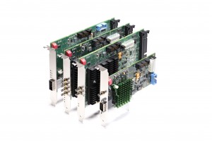
Riber produces MBE cells, accessories and service and OEM sources, but their most important products are their MBE tools that are used to deposit semiconductor thin films on substrate layers with a carefully controlled composition, thickness and electrical conductivity. These films form complex structures like LEDs, laser diodes, solar cells and transistors with properties not achievable with common silicon technology. Riber provides a broad range of innovative and high quality MBE systems designed for each main lines of compound semiconductors: III-V, Gallium Nitrides, II-VI and MCT, SiGe and new materials such as Graphene.
The company’s tools range from research reactors, used by leading research centers around the world, to larger production machines, which are operating in many of the world’s leading compound semiconductor foundries. Their machines include the Compact 21, a 3” MBE system, configurable for III-V, II-VI, Gp IV, Oxides, metals and GSMBE for fundamental research and device development; the MBE 412 with a 4″ (or 3 x 2″) capacity; the MBE 49 series, with a capacity of 200mm, 150mm, four 4-inch wafers or five 3-inch wafers, specifically designed for depositing arsenides, phosphides, nitrides and oxides. But their best seller is the 4″ / 6″ MBE 6000, which has become the MBE benchmark for high throughput & reproducibility. Finally, Riber provides solutions for passivation of laser facets and compound semiconductors - an important step in semiconductor processing. Their compound semiconductor passivation (CPS) reactor is designed to provide effective protection of surfaces or facets using various coating methods such as ZnSe, SiN and oxides.
The company’s main application fields are power & RF electronics, lasers, IR detectors, micro LEDs, passivation, emerging materials like graphene and superconductors, and solar.
The future
Jean-Louis is optimistic about Riber’s future growth. Firstly, many exciting applications are emerging for composed semiconductors. In the area of power & RF electronics, for example, GaAs/GaN-based devices are increasingly being used for RF transceivers for mobiles and 5G antennas. Similarly, VCSELs are finding new applications for 3D sensing, eye tracking applications and LIDARs for smart vehicles, and there has been a rapid increase in demand for thin-film technologies for the solar industry. Additionally, IR detectors based on mercury cadmium telluride, (MCT)) are used for LIDARs, night vision, surveillance and detection, while more recent IR detectors based on aluminium gallium antimonide are being used for gas sensing, medical applications, automotive and consumer electronics. There is also a booming demand for micro LEDs for next generation consumer displays. In this field, MBE has a major role to play because the process enables the easy incorporation of high indium fractions in gallium nitride, that covers the full visible spectrum without the need for phosphors or additional processing. Finally, a lot of research is being done on new materials such as topological insulator and superconductors. Although it is not clear if MBE can do better than CVD for 2D materials such as graphene, Riber sees superconductors as an emerging area and is currently developing a machine for the growth of material at very low temperatures (down to -200 °C) required by some crystal structures to produce superconducting material.
The growth strategy will be to move into silicon photonics, i.e., to make efforts to integrate III-V technologies and functional oxides onto silicon substrates in order to benefit from the existing equipment in silicon foundries. As a first step, Riber is developing a machine dedicated to growing a thin film of oxide on silicon. Hitherto, Riber have always made machines for providing epitaxial and not amorphous coatings, but in this venture the idea is to grow a functional oxide epitaxy on silicon to make it ready for a post epitaxy layer.
If you started again, what would you do differently?
“As regards Riber’s strategy, I’d go out into the market and engage with end users earlier - to share our vision, ensure we speak the same language and make sure we have the same end goals in sight.”
What’s your advice for the next generation of entrepreneurs?
“Don’t build you product in isolation and then show your customers the finished product. You need to go step by step; maybe it was good when you first started making it, but very often after testing, the customer will want changes. Always remember that the customer is key, and you will need to listen to them and make changes to your product to meet your customer’s exact needs.” My advice : understand the ecosystem, be part of it, work together to reach a WIN/WIN situation.
Written by Ivan Nikitski, EPIC’s Photonics Technology Program Manager