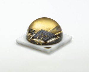
SCIL Nanoimprint Solutions offers solutions for making nano-structures on wafers by using its unique and proprietary lithography technology (SCIL). These nano-structures are used on optics and other photonic products to increase performance, lower end-product costs and increase functionality.
SCIL or Substrate Conformal Imprint Lithography is a cost effective, robust, high yield process enabling nanometer resolution patterns on a large variety of materials. SCIL delivers high quality imprints on wafer areas up to 300 mm. It can be used to make patterns with feature sizes down to less than 10 nm and overlay alignment below 1 µm.
In this article, Jose Pozo, EPIC’s CTO, talks to Rob Voorkamp, General Manager of SCIL Nanoimprint Solutions, a provider of solutions for high volume, high yield and low-cost imprint lithography for nanopatterning on full wafer-scale.
Early career
In 1990, Rob graduated with an MSc in Mechanical engineering from the Technical University of Eindhoven, and after 2 years of military service, he began working as a Project Manager for Gemco, a company providing design and engineering services to iron and cast metal foundries.
Then, in 1988, his former boss at Gemco, who had moved to Phillips, invited him to apply for a job at Phillips Components as an Industrial Project Manager. For the next two years, he worked on industrial restructuring projects for ferrite ceramic production until the division was sold to a Taiwanese company in 2000.
Having developed an interest in marketing and attracted by the idea of gaining experience in a new industry, he successfully applied for the post of Business Planning Manager with Philips Semiconductors. Initially involved in business planning and process improvement, a year later he became Product Marketing Manager, responsible for the marketing and design-in of discrete semiconductors for the big electronics companies, like Ericsson, Nokia and Siemens.
He stayed with Philips Semiconductors until 2005, when he moved to Royal Philips to take up the post of Director IP Licensing. At that time, Phillips were working on the idea of expanding business by enabling external companies to use their technology via licencing projects. As a result, they were looking for people who could Identify potential licensing opportunities for their technology among existing external companies as well as new start-ups.
From then on, Rob became heavily involved in the business development of Phillips’ high-tech technologies. This involved not only technology licencing, but also technology acquisition as he became increasingly involved in identifying new external technologies that could fill gaps in the company’s portfolio to cover new applications.
SCIL Nanoimprint Solutions
Through his search for licensing opportunities, Rob came into contact with Marc Verschuuren, a senior scientist at Philips Research, who had developed a new type of nanoimprint lithography that could be used in a wide range of applications.
The technology in question was Substrate Conformal Imprint Lithography (SCIL), a method for delivering high quality imprints on large areas up to 200 mm on a variety of substrates with nano and micro patterns down to less than 10 nm. Unlike conventional lithography processes, thanks to its soft conformal stamp, SCIL had fewer defects and caused less damage to the stamp materials. Patterns could be imprinted over particle contaminants with distortions dissipated in the soft rubber layer. The overall effect was Improved yield, lower operation costs and higher quality output.

Aware of SCIL’s market potential, Rob initially saw the technology as a candidate for a technology Licencing project. But after some positive feedback from some potential clients, he concluded that it would be a better idea for Phillips to develop the technology in-house. From a technology perspective, SCIL had the potential to become valuable for Phillips, and at a personal level, having spent a lot of his time enabling others to set up start-ups, this time he wanted to do it himself.
Convinced of the potential of the technology, Philips agreed to invest in the project. The result was the launch in 2015 of SCIL Nanoimprint Solutions, with Marc Verschuuren as Technology and Business Development Manager, Remco van Brakel as Operations manager and Rob as General Manager. Over time the venture grew to 12 people and more growth is expected.
Company development
Products: Over the last 5 years, SCIL Nanoimprint Solutions have developed three types of SCIL systems: the AutoSCIL, for fully automatic systems including all the essential process steps in a closed coupled system: wafer handling, pre-aligning, spin-coating, SCIL imprinting, baking and cooling; the FabSCIL, capable of imprinting 200 and 300mm wafers with automatic stamp loading and positioning; and the LabSCIL, a low volume SCIL tool especially developed for R&D labs and companies interested in small series pilot production.
Business strategy: As Rob explains, because their expertise was in materials and processes, from the outset, the company has aimed to be a technology solution provider, not an equipment manufacturer. As a result, their approach has been to determine the real needs of the customer and now these needs can be translated into the right process and the right materials. Accordingly, they have confined themselves to designing the equipment with the manufacturing contracted out to several expert manufacturer, such as VDL. In this way, the company has been able to maintain control over the hardware and focus on developing the consumables, i.e., process and materials. The advantage of this business model is once they have sold a tool there is recurring revenue coming from repeat orders for materials and processes, which is where their main strengths lie.
Materials: The materials consist of the stamp and the imprint materials. The stamp provides nanometre resolution patterns thanks to its tri-layer construction: the top layer, composed of X-PDMS (polydimethylsiloxane), carries the imprint structure, which is capable of fine detail, low pressure imprinting; the middle layer is composed of soft PDMS and the bottom layer comprises selected types of thin glass.
The imprint material comprises special inorganic, patented sol-gel resist material that is optically transparent, with a broad range of refractive indices, making it suitable for a wide range of applications from UV to IR. It is temperature stable, has good etch resistance and can be used both as a hard etch mask and as a functional layer.
In essence, a particular process is determined by the choice of stamp and the resist materials and how they are combined and tuned to work together to meet the needs of the customer.
The future
IP protection and logistics: One of the key issues for the company is how to protect the IPs relating to their processes and patented sol-gel resist material. A lot of time and know-how has gone into their development and most of the processes and materials are classified as Trade Secrets. For this reason, they intend to continue making the core materials in-house in order to minimise the risk of a competitor getting hold of the recipes.
Having said this, one of the problems with resist materials is that being temperature sensitive, they have to be transported on dry ice, which is both cumbersome and costly. As a result, they are thinking of working with partners able to manufacture the resits locally. One solution would be to ship the core ingredients, which can be transported at normal temperatures, and then have a subcontractor do the last part locally, subject to them signing confidentiality agreements.
Applications & markets
Rob's preferred future is for the company to become focused on a wider range of applications with a more or less standardised equipment portfolio so that they can tune the equipment to meet a range of specific customer needs.
As he points out, although nanoimprinting can be used in many applications, they are not targeting the semiconductor market. For him, it's all about optics and any applications that involve the manipulation of light, which is where they have the strongest offering. The key applications will therefore be in photonics, not only the classical technologies, like LEDs and lasers, but also optics for smart glasses, mobile phones, camera lenses, DOEs (diffractive optical elements) and metalenses - flat surfaces that use nanostructures to focus light in place of bulky, curved lenses currently used in optical devices. There's also a large opportunity for nanostructures in products like micro- and nano-LEDS.
Target markets include all those sectors that require ultra-high accuracy and quality optics, at affordable prices in the right volume, such as interior lighting for decoration and automotive, and AR/VR displays. However, as their SCIL technology is available and for mass production, an important target sector is the mobile phone industry – both the phone manufactures to create end-user interest, and also, more importantly, the companies producing the optical modules.
If you could start again, what would you do differently?
“To be honest, not a lot. I’ve really enjoyed the path I’ve taken, but if I started again, maybe I’d try to do something on my own earlier. Working for Phillips, I had the luxury of being able to pick from a candy box of great technologies the company was developing. But being younger I felt a bit insecure about taking the step to start my own venture. Of course, if I started again with the knowledge and experience I have now, I’d be a lot bolder.”
What are your words of wisdom for the next generation of entrepreneurs?
“First, it’s important to believe in yourself and the technology you’re developing. You need to listen to others, but in the end, you’ve got to make your own decisions and just go for it.
Second, you need to think about what makes your technology unique and then get it protected. I you don’t, before you know it, your technology will be out the door and someone else will be using it and undermining your competitive advantage. It doesn’t always have to be through a patent because processes are commonly known, and in any case, it can be difficult to prove what particular process a competitor has used. Another way to protect your IP is to classify your technology as a Trade Secret and get your business partners and employees to sign confidentiality agreements.”
Written by Jose Pozo, Chief Technology Officer at EPIC (European Photonics Industry Consortium).











 Back to Features