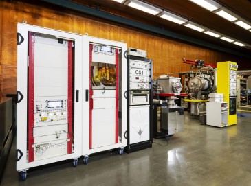


Rofin, a manufacturer of industrial lasers and laser systems, enters the semiconductor market with a turnkey solution for front-end-of-line (FEOL) processing. The new laser wafer-processing system Waferlase 200/300/450 is a fully automated modular platform comprised of a handling system for ultra-thin semiconductor wafers and a choice of laser processing modules, depending on the type of application. The Waferlase 200/300/450 product family starts with solutions for insulated-gate bipolar transistor (IGBT) laser-annealing and debris-free wafer-marking. Rofin will be showing Waferlase at Semicon West 2013 on 9-11 July at the Moscone Centre in San Francisco, California (US).
Rofin’s Waferlase 200/300/450 product family includes the following features:
• Wafer-handling technology: Rofin’s integrated wafer-handling technology to provide precise, non-contact transportation of ultra-thin wafers, even with considerable warp-age and bow. The system comes with two or more cassette ports for Open Cassette or Front-Opening Unified Pod (FOUP) wafer-carrier systems. Integrated scanners detect the position of the wafer in its carrier. The system software controls slot allocation, wafer warp-age measurement, wafer location and wafer identification (ID) detection; it would even change the pick-and-place sequence automatically in case of a wafer-damage threat (e.g., due to extensive or opposite bowing of neighbouring wafers). A high-end dual-arm robot handles wafer loading and unloading. The pre-aligner module centres and aligns the wafer. A “vacuum handshake” between the end-effecter and pre-aligner, including a wafer safeguard, secures damage-free handling of the wafer’s back side. Thus, the high-end technology and software control integrated in Rofin’s Waferlase 200/300/450 promises high throughput at negligible wafer-breakage rates.
• IGBT laser-annealing: The IGBT market is growing because of the advantages that IGBTs offer, such as high voltage capability, low ON-resistance, ease of drive, fast switching speeds and robustness. One of the key factors contributing to this growth is the increasing demand in automotive and industrial applications, including renewable energy, communications, medical, lighting and transportation.
IGBTs are manufactured on mechanically thinned wafers with a typical thickness of 100 micrometres (μm) or less. In order to establish a field stop or an emitter layer on the rear side of the wafer, deep-implanted doping elements, such as phosphorous and boron, must be activated through a high-temperature annealing process toward the end of the FEOL process chain. Often, the sensitive devices on the wafer’s front side are protected by an attached tape. Due to the low damage temperatures of the tape, the heat sensitivity of the front-side devices and a non-uniform heat distribution in the processing chamber, conventional oven activation is characterised by low activation levels and rates. Rofin’s laser-annealing process has been developed to overcome these issues and to provide high process stability and yield at competitive costs/wafer levels. Laser-annealing deep-activates the dopants and prevents damage to the wafer’s front side and the protection tape. The laser allows for precise depth control of the field stop and emitter-layer activation up to 2μm. Rofin’s IGBT laser-annealing solution has activation rates exceeding 90%.
• Wafer marking: Rofin’s Waferlase 200/300/450 systems produce traceable markings on transparent, semitransparent and opaque wafer materials. Two methods (i.e., hard and debris-free marking) are used; they differ in terms of process, depth and location of the mark. Debris-free marking in a clean-room environment is achieved by melting the silicon wafer’s surface.
Rofin’s new patent-pending marking technology allows the user to precisely control the marking depth ranging from less than 1μm to 7μm. The debris-free marking process uses a tailor-made integrated circuit (IC) marking laser source with a 532-nanometre (nm) wavelength. This dedicated solution achieves high contrast and performs well at small character heights.