

The latest silicon photonics breakthroughs by researchers at the University of Colorado Boulder, the Massachusetts Institute of Technology and Micron Technology Inc. could skyrocket the processing speed of electronics and, thus, preserve Moore’s law well into the future. The new microprocessors use light, not electrical wires, at extremely reduced energy consumption.
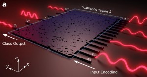
The team has created two different optical modulators, employing a technique that makes use of the existing microfabrication processes already used to build microelectronics. “We have figured out how to take the material layers on a silicon wafer that make up the transistor, the basic building block of microelectronics, and make instead an electro-optic modulator — a device that encodes electrical data onto a laser beam,” explains Milos Popovic, an assistant professor in the Department of Electrical, Computer and Energy Engineering at CU Boulder. The technique allows the scientists to guide the laser light in silicon nanowire waveguides on the chip and get the light off chip and to another chip via optical fiber cable.
“Since energy consumption is the bottleneck in scaling performance of microelectronics today, this will allow for the continued performance scaling of microelecronics into the immediate future, and at least temporarily a continued lease on life for one form of Moore's law, says Popovic, who led the research.
Photonics-based systems not only offer the advantage of greatly reduced energy consumption, they also enable packing a larger number of communication channels into a smaller space. Popovic explains that the speed of electrical communication over a wire is only a few gigahertz — “whatever the clock speed of the microprocessor is.” What is more, there is one communication channel per wire, and the wires connected must be placed at a minimum distance to avoid "crosstalk", which can cause noise and errors in communication. “In optics, first, you can have many communication channels on a strand of optical fiber — one channel on each color, or wavelength, of light,” says Popovic. “Second, the fibers can be placed very close together, as light does not have substantial cross-talk issues. As a result, a huge data bandwidth can be connected to and from a microprocessor chip to ‘feed’ the computation in cores of the CPU with data — data bandwidth that is simply unachievable in traditional electronics wire interconnects.”
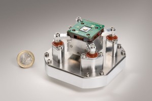
Two different optical modulators — SOI CMOS and bulk CMOS
Resonating light at particular wavelengths, the two optical modulators — one a disc, the other a racetrack — both allow light to propagate around them in a circular path. “When light at those wavelengths is incident on the resonator, it travels around many times and is absorbed, so nothing continues on and a 'zero' data bit is communicated forward,” Popovic explains how the photonics systems work. “When the resonator is detuned from the incident light wavelength, the light does not enter the resonator, and a 'one' data bit is communicated.” Both modulators accept data as a voltage, and the resonator shift translates it to the optical domain by. “The translation is done by producing an electron plasma in the silicon resonator, or depleting the electrons out of the resonator, due to the applied voltage, which causes the resonance shift,” Popovic explains.
Each modulator's design allows electrical contact and low optical loss in a structure formed from fully etched-through silicon. The difference is that the silicon-on-insulator (SOI) CMOS modulator is a disk with electrical contacts in the middle and light circulating on the outside, passing all the diode junctions. In the bulk CMOS modulator, on the other hand, junctions cannot be spaced so close together. The researchers, therefore, innovated a structure “where light wiggles between electrical contacts, avoiding contact with the metal, and thus optical loss, while ‘seeing’ all of the junction that causes modulation.” While the SOI CMOS design is more photonics-friendly and enables high-performance optical device, bulk silicon CMOS is the dominant industry process used by microelectronic and memory chip manufacturers, due to cost. “Hence, enabling photonics in bulk CMOS is something that can have enormous impact,” Popovic projects.
To get buy-in from the semiconductor industry, photonics scientists will need to show devices that can be incorporated into the microelectronics fabrication processes without major modifications. “That is what our current work demonstrates,” Popovic says.