A team of scientists from the Department of Energy’s Ames National Laboratory gained insight into a possible alternative material for solar cells. The team, led by Jigang Wang, senior scientist from Ames Lab, developed a microscope that uses terahertz waves to collect data on material samples. They focused on methylammonium lead iodide (MAPbI3) perovskite, a material that could potentially replace silicon in solar cells.
Terahertz range
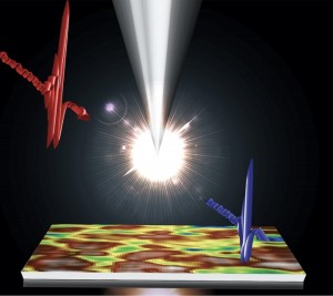
The way it works is that the microscope uses the terahertz range of electromagnetic frequencies to collect data on materials, explained Richard Kim, a scientist from Ames Lab. He said that the two features that make the new scanning probe microscope unique are that its range is far below the visible light spectrum, falling between the infrared and microwave frequencies. And secondly, the terahertz light is shined through a sharp metallic tip that enhances the microscope’s capabilities toward nanometer length scales.
“Normally if you have a light wave, you cannot see things smaller than the wavelength of the light you're using. And for this terahertz light, the wavelength is about a millimeter, so it’s quite large,” explained Kim. “But here we used this sharp metallic tip with an apex that is sharpened to a 20-nanometer radius curvature, and this acts as our antenna to see things smaller than the wavelength that we were using.”
In the paper published in ACS Photonics, the researchers describe the home-built THzSNOM setup as being made up of a laser, a vacuum and a cantilevered atomic force microscope (AFM). The laser is a femtosecond ytterbium laser with a pulse energy of 3 μJ, a repetition rate of 1 MHz, and a central laser wavelength of 1030 nm that can generate a bright source of pulsed THz radiation when applied to a nonlinear THz emitting crystal.
With silicon in short supply, scientists have been looking for alternate materials. The perovskite material MAPbI3 has been of interest to scientists as an alternative to silicon. A great benefit to perovskites is that they can transport an electric charge when it is exposed to visible light. The drawback for use in solar cells is perovskites degrade easily when exposed to elements like heat and moisture.
Insight into degradation problem
According to Wang and Kim, the team expected MAPbI3 to behave like an insulator when exposed to terahertz light. While they expected a consistent low-level of light-scatter throughout the material, they found, however, that there was a lot of variation in light scattering along the boundary between the grains, which gave them insight into the material’s degradation problem. Over the course of a week, the team collected data on the material, which showed the degradation process through changes in the levels of light scatterings. This information can be useful for improving and manipulating the material in the future.
“We believe that the present study demonstrates a powerful microscopy tool to visualize, understand and potentially mitigate grain boundary degradation, defect traps, and materials degradation,” said Wang. “Better understanding of these issues may enable developing highly efficient perovskite-based photovoltaic devices for many years to come."
The samples of MAPbI3 were provided by the University of Toledo. This research is further discussed in the paper “Terahertz Nanoimaging of Perovskite Solar Cell Materials,” written by Richard H. J. Kim, Zhaoyu Liu, Chuankun Huang, Joong-Mok Park, Samuel J. Haeuser, Zhaoning Song, Yanfa Yan, Yongxin Yao, Liang Luo, and Jigang Wang, and published in the ACS Photonics.









 Back to Features