


Veeco Instruments Inc. and ALLOS Semiconductors GmbH announced today the completion of another phase of their mutual effort to provide the industry with leading GaN-on-Silicon epiwafer technology for microLED production. The purpose of the companies’ most recent collaboration was to demonstrate the reproducibility of ALLOS’ 200 mm GaN-on-Si epiwafer technology on Veeco’s Propel MOCVD reactor when producing epiwafers for many prominent global consumer electronics companies.
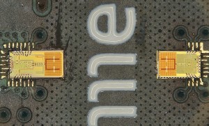
Sorting and binning are standard methods to achieve wavelength consistency for conventional LEDs. But microLEDs are too small and numerous to be sorted and binned; therefore, the uniformity of the epitaxial deposition is even more critical. The most important success factor for turning the promise of microLED displays into mass production reality is to achieve extremely good emission wavelength uniformity, which eliminates the need to test and sort individual microLED chips. Depending on the application and mass transfer approach, the target requirements of the industry are between +/-1 nm and +/-4 nm bin (min/max) on the epiwafer. Through this collaborative project, Veeco and ALLOS further improved the critical wavelength uniformity with the best wafer having a standard deviation of just 0.85 nm, representing an industry first on a production system.
Innovators in display technology are focusing on microLED as the next significant technological shift. According to research firm Yole Développement, the market for microLED displays could potentially reach 330 million units by 2025. This optimism is fueled by the promise of microLED technology (sub-100 micrometer edge length), which is considered the critical enabler to achieving the ultimate display with much lower power consumption. However, development of such displays has been hindered by high material costs and low yield and throughput of microLED mass transfer technology. This joint technical effort effectively addresses these challenges as Veeco and ALLOS continue to work with customers to further improve GaN-on-Si epiwafer and microLED mass transfer technology.
Veeco and ALLOS will showcase details of their breakthrough achievements at the International Workshop on Nitride Semiconductors in Kanazawa, Japan on Nov. 12, 2018.