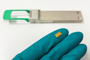


Researchers at the University of Sydney (Australia) used silicon CMOS technologies to design a new silicon photonics alignment and packaging system that could improve the manufacturing efficiency of biomedical and measurement sensors and, thus, reduce cost.
“By taking advantage of the superior properties of a laser, it was possible for us to create a unique lensless system for accurately detecting nanoscale movements of an optical fiber in real time,” says Keith Powell, a research honors student under the wings of Professor Xiaoke Yi in the University’s School of Electrical and Information Engineering. “This new technology enabled us to design the first fully autonomous alignment system in its class, offering faster alignment, more compact size and minimal setup at a significantly reduced cost.”
Reducing the cost of silicon photonics alignment and packaging
Powell blames high manufacturing costs for the fact that silicon photonics devices are still not widely adopted, despite many of the benefits they provide for telecommunications, biomedical and defense. He explains that a significant part of this cost is due to the alignment and packaging of the optical I/O. “Our unique technology can significantly reduce the cost of alignment and packaging by removing the need for a technician to operate or perform manual alignment of each chip. Our design can easily be integrated into a mass production line for high volume production of silicon photonics devices, allowing lower prices to be available to the market.”
The key application for this new closed-loop system would be silicon photonics alignment and packaging. “However,” says Powell, “applications could extend to wire bonding and potentially early detection of land slides and earth quakes due to the uniquely high sensitivity of our device to nanometre movements.”
Furthermore, the technology could also increase the efficiency, consistency and scalability for massive packaging of photonic Inter Circuit (PIC) chips, which are primarily used in fibre-optic communication, biomedical and photonic computing. Other uses could include radar, antenna, optical interconnect and nanophotonic packaging.
For the future, the team plans to move from the prototype phase into a production phase. “We believe our technology is suitable for developing a small-size and portable photonic alignment and fiber bonding machine for use in research labs and industry,” Powell says. “The form factor would be similar to existing high end fiber splicing machines.”
Written by Sandra Henderson, Research Editor, Novus Light Technologies Today