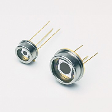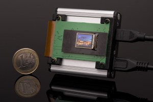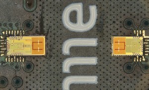


Soldering image sensors directly to the PCB can be a very risky and expensive practice in terms of damaging the color array during soldering, scratching the glass cover during cleaning, blistering the PCB when de-soldering a faulty device, and more. With image sensor sockets from Andon Electronics, global imaging expert Framos provides a unique and cost-effective solution.
For camera OEMs and their EMS suppliers, the higher melting point of today’s lead-free (versus tin-lead) solders presents an increased risk of heat-related damage to any image sensor soldered directly to the PC board. Likewise, the higher temperature required to de-solder a faulty or obsolete device increases the risk of damage to the PC board.
Heat is not the only risk factor associated to mounting devices directly onto the PCB. Harsh cleaning solutions can scratch the sensor’s glass cover – whose clarity is essential to the proper functioning of the camera.
The resulting yield losses – depending on the cost of the device, the frequency of device or board damage, and the labor required to manually solder or de-solder the image sensor – can substantially erode profitability and compromise lead times.
Soldering image sensors directly to the PCB also means holding up the start of PCB assembly until the devices arrive. The resulting expansion of lead times can compromise competitiveness, customer satisfaction, and sales figures. You can reduce this impact by keeping higher device inventories, but that ties up cash.
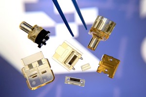
As the inventor of numerous precision high-reliability sockets for military, aerospace, medical, and commercial use, Andon Electronics has a long history of helping companies protect against device yield losses. Andon’s unique SENSTAC sensor socket contact was developed for military- and aerospace-grade high temperature/humidity/shock/
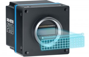
Andon’s broad socket line accommodates a wide variety of LCC, PGA, BGA, and DIP footprints utilized by leading image sensor brands like Sony, ON Semiconductor, Aptina and Truesense.