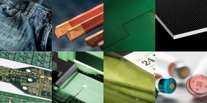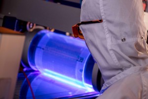
Stensborg has been a pioneer for 20 years in nanoimprinting lithography solutions for research institutions and industry. Jose Pozo, EPIC's CTO, interviewed CEO Jan Stensborg about the development of this privately held Danish company, its technology and the future of nanoimprinting in important application areas.
Early career
Originally trained as a toolmaker, in 1982, Jan joined the Royal Danish Navy, where he specialised in deep sea diving, explosives and search and rescue for fishing boats in the north Atlantic especially around Greenland.
During this period, he became fascinated with holograms and the potential of lasers to provide 3D visualization for deep sea diving particularly for oil platforms. Accordingly, on leaving the navy in 1987, he retrained at the Holographic Laboratory, a spin off from the Technical University of Denmark. For the next 10 years, he worked with various research groups on holography and interferometry, a technique that uses the interference of light waves to measure distances with great accuracy. In the early 90s, Jan started working with companies like Bang Olufsen and Lego and other Danish companies who were beginning to see the benefits of interferometry for testing product integrity, Head-Up Displays (HUDs) and counterfeiting applications.

They also worked with various forms of embossing and injection moulding and teamed up with researchers and companies working on nano imprinting producing CDs and DVDs. Then, in the mid-90s, following IBM’s lead, they started to experiment with Polydimethylsiloxane (PDMS) for making nano imprints on opaque substrates.
The creation of Stensborg A/S
With the aim of using the experience and expertise Jan and his team had accumulated over the previous 10 years, Stensborg A/S was created in 1998 to assist companies to implement nano imprint lithography and maximize its utilization.
Technology: By 1999, it had become apparent that the then current techniques and materials for nanoimprinting had a number of limitations, Firstly, infrared heating and hot embossing had several drawbacks and there was a need for UV curable materials. Secondly, while PDMS was good for what IBM had invented it for, the material was too soft, and resins diffused up into the polymer making it unsuitable for imprinting.
At the same time, there was growing demand from governments and the banking industry for high-volume security and anti-counterfeiting printing solutions, which required a technique for volume nano imprinting on opaque substrates using UV curable materials.
As a solution, Stensborg came up with a ground-breaking imprint technique - the Holoprint® that enables users to imprint high-resolution, three-dimensional (3D) nano surface relief structures directly on their pre- or post-printed web material, without the need for using any prefabricated foils.
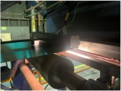
Over the next 15 years, Stensborg developed two innovative nanoimprint lithography (NIL) methods based on their patented technology. The first, was the Roll-to-Roll (R2R) method used for volume fabrication on flexible materials including paper, and polymers. For this method, which was first introduced in 2010 in Germany, Stensborg developed its own unique and patented nip moulding process designed for nanoimprinting on transparent as well as opaque materials. The advantages of this approach are that it avoids costly and undesirable web coatings, allows in-line partial register nanoimprinting, reduces costs and the manufacturing process due to a partial layout of an active nanoimprint area, and has a positive environmental impact due to the speed of production and low energy consumption.
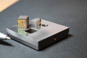
The second method was Roll-to-Plate, which is an imprinting process consisting of a roller mechanism and a rigid surface plate. This technique, first introduced in 2016 in Austria, is better suited for the production of non-flexible substrates, e.g. glass and quartz and is the preferred method for prototyping optical masters as it allows the production of smaller quantities, lowering the time consumption while minimising waste. This is an ideal method for experimenting and testing new nanoimprinting topologies before mass production. Its main advantages are that it imprints a micro -or nanostructure in a thin nip line, and auto-compensate for substrate unevenness, and enables a method for fast sample making as well as providing a tool to establish parameters for future Roll-to-Plate upscaling
Thanks to Stensborg‘s pioneering work, it is considerably easier nowadays to solve nanoimprint lithography problems in volume than it was 20 years ago. In fact, it is no exaggeration to say that the current nanoimprint lithography industry is indebted to Stensborg‘s cutting-edge nanoimprint lithography solutions developed over the past two decades.
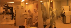
Products: Stensborg has expanded to become a fully-fledged facility with cleanroom facilities, chemistry development, and production of optical components. The company currently offers 4 types of products: 1) Launched in 2019, the Holoprinter Uni A6 DT is a portable and affordable solution to provide research institutions with an easy-to-use product for small-scale nanoimprint, roll-to-plate manufacturing lithography work.
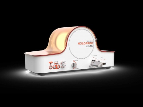
This desktop device is ideal for prototyping, testing and characterising materials and processes for applications such as diffractive optical elements, holographic optical elements, hydrophobic topologies and lab-on-chip devices; 2) a range of consumables for nanoimprint lithography, such as master template UV resins and light-curing resins; 3) volume production using R2R and R2P manufacturing, e.g., for diffractive optical elements, optical waveguides, and holographic optical elements; 4) Custom-made services to fit their customers’ specific needs, from light-curing resin to equipment modifications and bespoke custom-made machinery and chemistry.
Enabling future volume production
Regarding productss, Jan is optimistic that their Holoprinter Uni A6 DT will be good for future business, not only from sales revenues but also because of its potential to enable future volume production. University researchers and private research labs are provided with a desktop device they can use to quickly test and develop new nanoimprinting topologies. As Jan points out, young students can come up with some very smart ideas for new applications, e.g., in the energy, medical and communication sectors and new sensing methods that can’t be done with traditional technologies. Stensborg can assist where there’s business potential to scale to high-volume production.
For volume production, there are currently 5 main growth areas.
Micro-optics: Since 2018, there has been growing interest in micro-optics from larger corporations and fortunately major new developments will help servicing these corporations through : 1) the supply of custom optical masters from companies like SPIO Systems ApS and NIL Technology ApS; and 2) latest developments in the industry for making master topologies.
Medical: The second growth area is the medical sector, specifically, for microfluidics and topology enhancing applications, for example, for DNA analysis and point of care diagnostics.
Solar energy: There is growing interest in Europe for the production of solar energy, and in this connection, Stensborg has already delivered nanoimprint solutions to improve functionality in flexible solar cells as well as solar concentrators. Another growth area in the solar market is the colouring of both rigid and flexible solar cells to make them more aesthetically pleasing for city planners and architects. The challenge is how to add colour without degrading efficiency, which Stensborg is currently addressing by modifying topologies.
Communications: Another growth market is optical communications resulting from a greater use of polymers and optics, e.g., making part of a lens in a polymer and part of it in glass. The advantages of polymers over glass are that while they have the same optical quality, they are faster to process, hence more price competitive and can open up for new market applications.
Free-form micro-optics: Finally, in recent years, there has been an explosion in free-form micro-optics. These are micro-optical components designed with no symmetry constraints which gives them improved performance over traditional micro-optic imaging systems. Applications include augmented reality (AR) displays, commercial and consumer lighting, and solar panels. Ultimately, Jan sees a time when glasses are available that enable the wearer to ‘see’ and adjust both visible and non-visible light.
If you started again, what would you do differently?
“I’ve got no regrets. Looking back, it’s always possible to think that something could have been foreseen. But, having said that, I think I would trust my instincts to a higher degree and be more proactive when I see the potential for a particular technology. For example, the potential for diffractive optical elements for medical applications was apparent several years ago, but I, like many others, did nothing about it because it was too cumbersome to convince the industry.”
What are your words of wisdom for the next generation of entrepreneurs?
“First, find something you’re fascinated about and study the topic as much as you can. Second, learn as much as you can from others and trust your instincts when moving beyond. Third, don’t be afraid of sharing your ideas; getting feedback is important and if someone copies you, take it as a compliment.”
Written by Jose Pozo, Chief Technology Officer at EPIC (European Photonics Industry Consortium).


















 Back to Features