


In this interview, Antonio Castelo, EPIC’s Technology Manager for Bio-Medical and Lasers, talks to Celia Millon, Founder and CEO of RayVen, a supplier of 2.1 µm SWIR ultrafast lasers for industrial applications.
What’s the background to you founding RayVen as CEO?
In 2015, after completing a BSc and then a Masters in Physics, I started a PhD at French Alternative Energies and Atomic Energy Commission, where I worked on non-destructive testing using laser ultrasound for additively manufactured parts. After my PhD, I went to École Polytechnique as a postdoc for 12 months, working on ultrafast laser filamentation and nonlinear optics.
Then, in 2020, I moved to Germany to do a second postdoc at Ruhr University in Bochum, working on high-average-power terahertz sources, water spectroscopy, and ultrafast laser technologies.
 I was in contact with a lot with other postdocs working on lasers developing a 2.1 µm ultrafast solid-state laser in the group of Prof. Saraceno. Traditionally, 2-µm ultrafast lasers were limited by thermal management issues, and low average power. But by integrating optimised Tm/Ho gain media with a carefully engineered chirped-pulse amplification architecture, they managed to solve these issues and created a 2.1 µm high-average-power ultrafast output with improved beam quality, efficiency, and stability.
The fact that 2.1 µm lasers could now be engineered into practical systems enabling low-damage processing, created a lot of interest among companies and other research groups. This convinced us that the technology had commercial potential and we began to think seriously about creating a start-up. I spent the next 12 months talking to potential customers to determine the right applications. Finally, having received positive feedback, we registered RayVen in March 2025
What products have you developed?
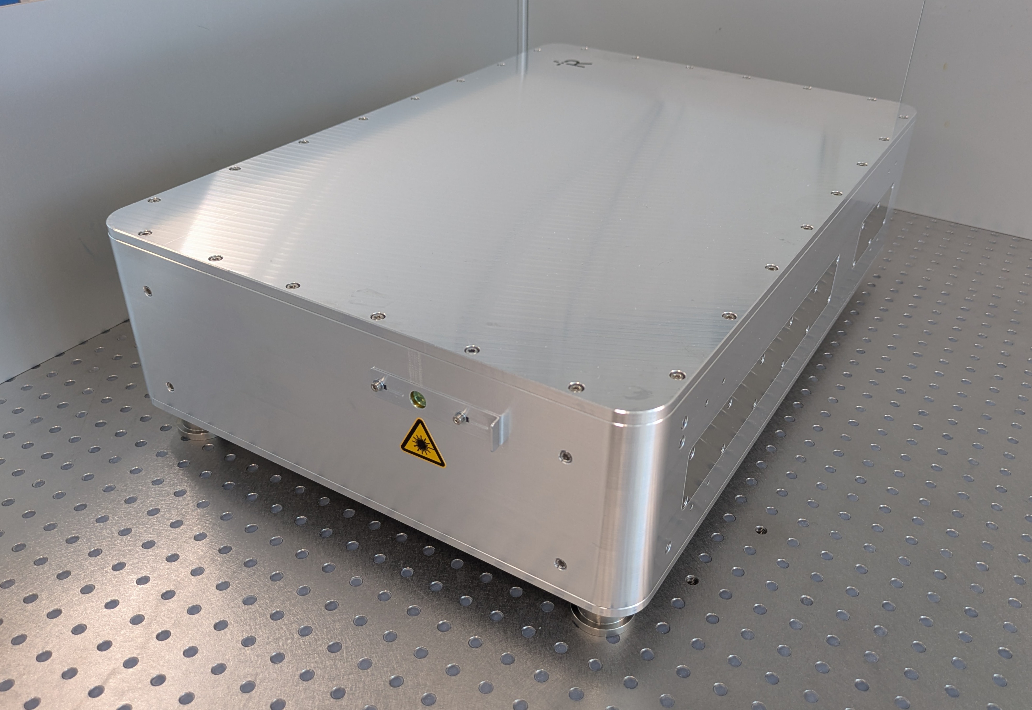
We now have two products. The RayVen-S 2.1 µm is an ultrafast oscillator that provides 1 W of average power at a 50-70 MHz repetition rate, with 120 fs pulse durations across wavelengths from 2090 nm to 2120 nm.
Our other product is the RayVen-L 2.1 µm, an ultrafast amplifier system that can deliver up to 1 mJ of pulse energy with 1 ps pulse duration.
What are the main applications?
Our applications are in three areas: glass, e.g., writing waveguides; polymers, e.g., microstructures for lab-on-chip devices for biological analyses; and semiconductors. Of these, our main focus is on semiconductors because our lasers can significantly enhance material processing for the semiconductor industry.
Because 2 µm light penetrates silicon with minimal surface absorption, our lasers can write structured layers directly inside silicon wafers. This capability enables precise internal modification of silicon without damaging the surface, which is increasingly important for advanced semiconductor manufacturing.
In addition, the photon energy at 2 µm lies close to germanium’s bandgap, allowing highly precise subsurface processing of germanium within complex chip architectures. This makes such processes compatible with integration into CMOS manufacturing flows.
RayVen’s lasers also enable the fabrication of vertical electrical interconnects through silicon, known as through‑silicon vias (TSVs). These interconnects support 3D stacking, significantly improving device performance, reducing power consumption, and enabling more compact and advanced semiconductor systems. Furthermore, our technology can be applied to wafer bonding and debonding, allowing controlled modification of interfaces and internal layers within wafer stacks without damaging the surrounding device structures.
How have you gone about finding potential customers?
Because our technology is not widely known, I’ve had to engage in “technology push” i.e., promoting our three main USPs (2.1 µm high-power ultrafast performance, compactness, and stability) and finding markets and customers where it can be applied.
To this end, I’ve attended trade fairs, conferences, webinars, and EPIC meetings and workshops to identify potential customers, discover their needs and problems and determine how our technology can benefit them.
Simultaneously, we’ve delivered our laser systems to pilot customers and development partners in research labs and industrial R& D teams, so we can see how our technology works in real-world conditions and get feedback to refine our products. We also have our own R&D to do feasibility studies. Customers can come with their samples and we assist them on the use of the laser and share the results.
What have been your main challenges?
On the technical side, although building lasers was not one of my core competences, my PhD experience in additive manufacturing and laser ultrasonic systems has made me adaptable. So, boarding on the basics of laser manufacturing and laser processes has not been too difficult.
My biggest challenge has been transitioning from a scientist mindset to a CEO mindset -having to deal business management and the difficult area of recruiting and retaining talent. There’s no textbook for that, and I'm learning every day. My main strategy has been to surround myself with the CEOs of other laser companies and use them as mentors, as well as attending EPIC sessions, where members can get expert help and advice.
As a woman, have you found any challenges working in a sector populated predominately by men?
In my experience, women often adopt communication styles that are more measured, collaborative, and less confrontational. This is what society expects. While these approaches are entirely valid, they can sometimes be less effective in highly competitive situations, such as investment discussions or contentious decision‑making environments. The challenge is therefore less about gender itself and more about how individuals are perceived and how their messages are framed in such contexts.
Over the past 10 years, initiatives to promote women in photonics have increased women’s participation to around 25%, although leadership representation remains significantly lower at about 11%. For this reason, professional programmes, e.g. IEEE, targeted workshops, industry diversity policies, aimed at accelerating the progression of women into senior roles are crucially important.
How do you see the future in terms of market growth and the competition?
The temperature of 2 microns has changed a lot. Last year, at Photonics West, people were lukewarm. But this year, many integrators came to me and said, “You know what? My customer wants 2 microns. Can we chat?” So, the market is definitely picking up.
Of course, there are regional differences. It’s easy to collaborate in Europe, but Asia is a lot more difficult. In Japan and Korea, for example, customers want you to have a perfect outstanding product immediately available, and they prefer to go through a distributor rather than talking directly to the laser manufacturer. This can be problematic because it’s sometimes difficult to know if the distributor fully understands the advantages of our technology and is able to deliver the right message to their customers. This is not an easy game and it's also time consuming.
For these reasons, I think it will take a couple of more years to reach to the point where we can integrate our lasers into semiconductor manufacturing companies.
As regards competitors, although 2 micron is still a small market, there are many niches that cannot be all covered by one company. We all have different customers and specific applications so we sometimes collaborate – exchanging ideas on company specific applications, which in our case are wafer bonding/debonding and TSVs.
What advice to you have for the next generation of entrepreneurs?
First, be bold and authentic. In a rapidly changing world, the idea of complete safety is largely an illusion, and progress often requires taking calculated risks.
Second, engage early and actively with the ecosystem. Attend conferences, webinars, and trade shows as soon as possible to showcase your technology, speak directly with potential customers, and understand their needs so you can clearly articulate how your solution adds value.
Third, become involved in industry associations such as EPIC. These networks provide access not only to customers and collaborators, but also—crucially—to experienced mentors who can offer guidance at key stages of your entrepreneurial journey.