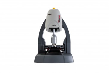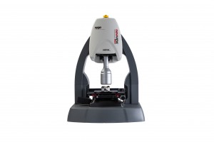


Laser Components’ partner Optometrics Corporation in Littleton, Massachusetts (US), recently added advanced scanning atomic force microscopy (AFM) within their metrology capabilities, with the aim to enable new benchmarks for nano-scale measurement, characterization and manipulation for diffraction grating design optimization.
When diamond ruling or holographically recording a new master grating, inspection through advanced high-resolution imaging tools provides confirmation that the shape and pattern of the microscopic groove has been optimized and produced as designed.
Diffraction efficiency and dynamic range are critical parameters in many spectroscopic instrument designs. Understanding why a particular diffraction grating may have a small yet necessary performance differentiation for instrument design success can be crucial.
For instance, many diffraction gratings are simply referred to by their original production method, groove frequency and blaze, such as ruled 600 line/mm 400 nm. Yet, not all ruled 600 line/mm 400 nm gratings are alike. Similarly named “masters” may actually vary depending upon the potential size, shape and location of unintended anomalies on the individual master diffraction grating groove facets. These nanometer-scale differences may noticeably impact performance over narrow or broad spectral regions.