


Designers that want to use Infinera InP open foundry services, part of the Infinera Optical Innovation Center, will now benefit from a new design workflow that starts from a graphical photonic integrated circuit design and system simulation environment. This workflow is enabled by the new VPItoolkit PDK Infinera — a pluggable toolkit extension to VPIcomponentMaker Photonic Circuits by adding support of the Process Design Kit (PDK) building blocks for the InPbased PIC foundry process offered by Infinera. VPIphotonics and Infinera collaborated to develop compact models for the PDK building blocks based on the characterization data of the individual devices and the test measurements of fabricated chips.
The foundry capability was developed in collaboration with AIM Photonics and the US Department of Defense. This ensures that each building block is represented by an adequate simulation model with only a few parameters to control. A designer can rapidly prototype application-specific photonic integrated circuits with prerequisite functionality without going deep into the details of device layout and fabrication process. Once the design is completed and optimized, the schematic can be exported to a netlist and passed to Infinera’s InP foundry for physical layout implementation, careful verification, and fabrication.
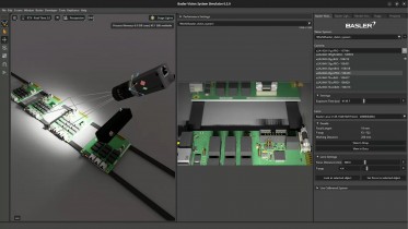
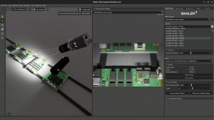
All the building blocks available in VPItoolkit PDK Infinera can be used alongside with a broad set of standard modules and instrumentation available in VPIphotonics Design Suite, especially VPIcomponentMaker Photonic Circuits (circuitlevel design and analysis) and VPItransmissionMaker Optical Systems (system-level evaluation). Hierarchical circuit designs and advanced parameter scripting, sweep and optimization of parameters, sensitivity and yield analysis as well as systems benchmarking and characterization are supported transparently for designers helping to increase their productivity.
Given Infinera’s experience with manufacturing highperformance PICs, the foundry PDK offers fully optimized devices to ensure optimal performance and yield within the foundry’s integration platform [1]. The capability of embedding these building blocks into the VPIphotonics software framework enables the simulation and modeling of complex photonic integrated circuits with a high degree of reliability.
Visit VPIphotonics team at Photonics West 2020 on Feb 4-6 in San Francisco at booth 3173 for more information and live demonstration.