


Researchers at the National Institute of Standards and Technology (NIST) in the US have expanded on their previously developed technique for improving optical microscopes, now applying it to monitoring next-generation computer chip circuit components. The technique, called through-focus scanning optical microscopy (TSOM), could prove essential in developing 3D computer chip components.
“The TSOM method makes use of the 3D optical data acquired using a conventional optical microscope for 3D shape analysis of micro- to nanoscale targets,” explains Dr. Ravikiran Attota, TSOM project leader at NIST. Providing sub-nanometre measurement sensitivity in all three directions (X, Y and Z), the TSOM technique can detect and measure the “nooks and crannies” in the three-dimensional shapes of circuit components that a light beam could otherwise not reach (a limitation that renders conventional optical microscopy methods inadequate). TSOM’s level of sensitivity, thus, could resolve measurement challenges in the manufacturing of next-generation 3- computer chips.
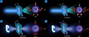
Attota explains that with the TSOM method, three-dimensional optical data is collected by stepping — or scanning — the target along the focus direction and acquiring optical images at each step location ((a) in the illustration). Stacked through-focus optical images form 3- optical data (b). And finally, as illustrated under (c), “A convenient way to visualise and analyse this 3- data is to extract an image along a vertical cross section passing through the location of interest on the sample (through the centre of the nanoparticle, for example) as a 2- TSOM image,” Attota demonstrates. “In the TSOM image, the X (horizontal), Y (vertical) and colour scale axes represent the spatial position across the target, the focus position and the optical intensity, respectively.”
In addition to showing potential in measuring the increasingly smaller 3D structures of advanced computer chips, the TSOM method also has the ability to minimise or eliminate cross correlation — or “cross-talk” — for different dimensional changes, as Attota explains. Hence, the method “shows promise as a process or quality control tool for nano-manufacturing.”
In fact, the expert agrees that his team’s research advance could help transform the semiconductor industry. “3D structures such as FinFETs, HAR (high-aspect ratio) and TSV (through-silicon vias) are increasingly being used in the semiconductor industry,” he says. “It is challenging to find a non-destructive and high-through put metrology method for these 3D structures, and the TSOM method shows promise for such applications.” Moreover, the TSOM method is economical, as it only requires an optical microscope. Optical modelling, which is a “complicated” process, according to Attota, is also not needed for process control.
The research is detailed in the paper “Critical dimension metrology by through-focus scanning optical microscopy beyond the 22 nm node,” published in Applied Physics Letters.
Written by Sandra Henderson, Research Editor, Novus Light Technologies Today