AlixLabs AB, a Swedish semiconductor startup specializing in Atomic Layer Etching (ALE), announces its expansion into the photonics field thanks to a new research grant from the imec-led and EU-supported PhotonHub Europe. The total value of the research project is approximately 197,000 euro, of which PhotonHub will provide 58,500 euro, with AlixLabs itself investing 129,000 euro.
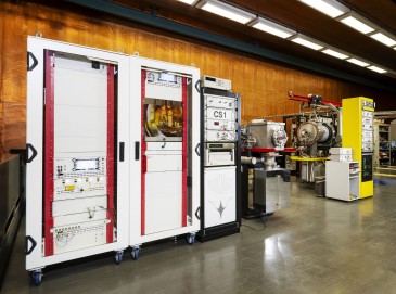
The R&D project with PhotonHub Europe will allow for AlixLabs to work closely with the European Union’s most prolific semiconductor research hub imec, granting access to photonics equipment and technology not present at AlixLabs’ headquarters in Lund, Sweden. The project also enables AlixLabs to evaluate, prototype and benchmark its technology and processes in imec’s laboratories, qualifying them for worldwide industry use.
“Photonics is a hot topic in the future of semiconductor industry, and we are eager to explore application of our technology in this field,” said Reza Jafari Jam, Research Director at AlixLabs. “We’re thrilled about the opportunity to collaborate closely with imec and tap into the vibrant hub of European semiconductor research, enhancing our capabilities in developing high-performance photonic devices. Our passionate team is looking forward to pushing the technology’s boundaries with our innovative solutions and contribute to better communication, computing and medical technologies.”
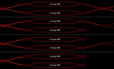
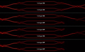
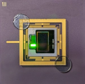
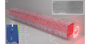
The goal of the project is to significantly enhance the performance of photonic devices, particularly ring resonators. With AlixLabs’ ALE process, which allows for precise material manipulation at an atomic scale, the goal is to achieve defect and damage-free surfaces for photonics devices. As surface quality directly contributes to better photon extraction and transmission, ALE in photonics is expected to result in more reliable devices with higher signal quality and enhanced operational qualities.
PhotonHub Europe was announced in 2020 and is funded by the EU’s Horizon 2020 program. It has 54 partners and over 500 experts from 15 EU member states, all aiming to create and launch new products in industries as diverse as Health, Digital Infrastructure, Manufacturing, Safety, Security, Space & Defence, Agro-Food and Mobility & Energy.
Established in 2019 in Lund, Sweden, AlixLabs emerged as a spin-off from Lund University with a mission to enable the cost-effective and energy-conscious fabrication of semiconductors, particularly logic and memory components. AlixLabs boasts patented recognition for its groundbreaking APS technique, a process that achieves nanostructure division through etching. This method holds approved patents across the USA, Taiwan, and Europe. The APS acronym signifies ALE Pitch Splitting, leveraging ALE (Atomic Layer Etching), a plasma-based dry etching cyclic methodology.











 Back to News