Researchers have demonstrated a new multi-functional device that could help advance the scalability of solid-state color centers, enabling them to be used in larger and more complex quantum computers and networks. As efficient photon-spin interfaces, solid-state color centers are promising candidates for qubit nodes — essential units for storing and processing quantum information.
Solid-state color centers are point defects that can absorb and emit light at specific wavelengths. To be useful in real-world quantum applications, they must be optically addressable in a fast and controllable manner while also allowing fine tuning of their optical transition frequencies and coherent spin manipulation. The new device enables all these functions simultaneously within a scalable and cryogenically compatible platform.
D. Andrew Golter from the MITRE Corporation will present this research at Frontiers in Optics + Laser Science (FiO LS), which will be held 23 – 26 September 2024 at the Colorado Convention Center in Denver.
“Future large-scale quantum technologies will require building blocks that include all necessary functionality, while also holding the potential for massive scalability,” said Golter. “We believe our work is an important step toward engineering these building blocks.”
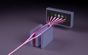
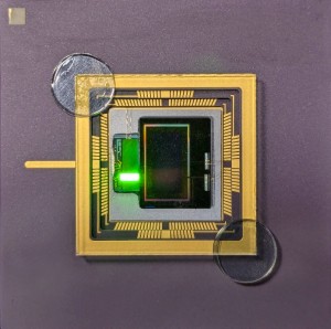
Working under the auspices of MITRE’s Quantum Moonshot program, researchers at MITRE, MIT, Sandia National Laboratories and The University of Arizona designed a cryo-integrated system-on-chip device that contains tin vacancy color-centers whose optical emission is coupled to diamond nanowaveguides on the chip. The qubit’s optical and spin transitions can be tuned and manipulated through integrated microwave lines, which can manipulate the qubits’ quantum states, and strain actuating cantilevers, which can be used to change the electronic and optical properties of the spin centers. Additionally, a multi-channel atom-control photonic integrated circuit that features high-speed piezo actuation supplies programmable independent optical excitation for multiple qubits simultaneously.
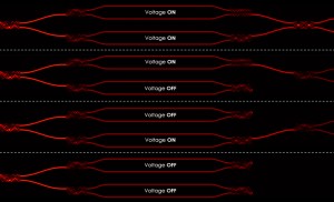
The researchers show that each output channel of the atom-control photonic integrated circuit achieves high extinction (> 35 dB) and high-speed (> 30 MHz) optical switching with very little crosstalk between channels. The results indicate that the new device can be used for high-fidelity strain and microwave control over multiple qubit nodes that are coupled to independent optical excitation and collection channels.
“We are working now to integrate these color center qubit control devices together with on-chip photonics, with the goal of achieving a truly scalable platform for quantum information processing,” said Golter.
About Frontiers in Optics + Laser Science
Frontiers in Optics, the annual meeting for Optica is presented with Laser Science, the annual meeting of the American Physical Society, Division of Laser Science. The two meetings unite communities from both societies for comprehensive and current research in a diverse collection of optics and photonics topics and across the disciplines of physics, biology and chemistry. The 2024 FiO LS Conference will feature hundreds of live contributed and invited talks. More information at https://www.frontiersinoptics.com.
About Optica
Optica, Advancing Optics and Photonics Worldwide, is the society dedicated to promoting the generation, application, archiving and dissemination of knowledge in the field. Founded in 1916, it is the leading organization for scientists, engineers, business professionals, students and others interested in the science of light. Optica's renowned publications, meetings, online resources and in-person activities fuel discoveries, shape real-life applications and accelerate scientific, technical and educational achievement. Discover more at: Optica.org
CAPTION: a) Schematic of the APIC and SoC. i) APIC. ii) SoC. Diamond waveguides are positioned on piezo actuated cantilevers and over a MW line. Optical excitation with multiple beam spots occurs perpendicular to the chip. One end of the diamond waveguides couples to on-chip SiN waveguides. b) Calibration plot of transmission, demonstrating high extinction on one of the APIC channels. c) Pulsed transmission from an APIC channel demonstrating high-speed operation. d) Microscope image of 4 beam spots on the SoC. Each spot can be independently modulated by the APIC and steered by an SLM. CREDIT: Andrew Golter, MITRE Corporation







 Back to News