


“NIL has already been implemented for some non-semiconductor applications, mostly at the research level,” explains Amandine Pizzagalli, Technology & Market Analyst, Semiconductor Manufacturing at Yole Développement (Yole).“Semiconductor devices mostly require photolithography technology. However, the emergence of new semiconductor devices demands tighter nanoscale resolution, complex shapes and more cost-effective lithography solutions. This has triggered the need for new patterning processes.”
Although the NIL equipment business is still a niche market for semiconductor applications, it is expected to explode. Its CAGR between 2018 and 2024 will reach an impressive 24%, making the market worth US$146 million by 2024, announces Yole in its Nano-Imprint Technology Trends for Semiconductor Applications report.
The NIL report from Yole is a detailed analysis of the technologies in three major semiconductor applications: photonics, biochips and front-end memories (3D NAND). It details the key players and supply chain and announces 2018-2024 equipment market forecast (breakdown by device type and end-application segment). This market & technology report also presents the equipment suppliers by device type and global market shares within the semiconductor business. Yole’s analysts also deliver an overview of the NIL technology users and a detailed roadmap related to the technology adoption.
What are the main NIL technologies for semiconductor applications? What is the status of NIL adoption today? How will it evolve? What are the key drivers? What are the remaining challenges for NIL implementation? How is doing what? The market research & strategy consulting company is offering today a comprehensive overview of the NIL technologies applied to the semiconductor applications.
The semiconductor industry is therefore regaining interest in NIL, which is based on mechanical replication.
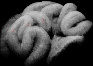
The technology is especially relevant to photonic elements, biochips and front-end 3D NAND memory, as it enables nanoscale structures below 20 nm over large surfaces and provides complex patterning capabilities.
On the photonics side, NIL technology realizes complex pattern shapes in a periodic way. For life science, the same technology ensures biocompatibility and solves the challenges of increasing complexity of biotechnology devices while enabling finer feature sizes. In the memory business, NIL could represent a cost-effective solution to achieving high-resolution feature sizes.
However, there are still some big barriers that prevent NIL from entering mass production. Generally speaking, the master fabrication process appears to be a critical step that increases CoO of the NIL process. Additionally, stamp lifetime and finding a trade-off between overlay, defect levels and throughput are issues that are holding back of NIL in high volume manufacturing.
Solving all these limitations could be a game-changer for NIL in the semiconductor industry.
Excitement about NIL technologies has grown exponentially since 2014, when Canon completed its acquisition of Molecular Imprints, a start-up provider of nano-patterning systems for the hard disk drive and semiconductor sector.
“Numerous companies with different business models have now invested in NIL technology,” comments Amandine Pizzagalli from Yole. “Including photonic element manufacturers, epi-house foundries, microfluidic foundries or integrated device manufacturers, applications span AR , 3D sensing and datacom/ telecommunications. This paves the way for a significant boost to NIL.”
Increasing demand for lower cost lithography solutions, integration of complex shapes and patterns and nanoscale structures is expected to offer many opportunities for NIL technologies. This will drive the NIL equipment market in the next few years.
So which semiconductor devices will revive NIL into the next-game changer?
For which applications will NIL be used? Currently, the real boost for the NIL equipment market is expected in photonic elements, driven by AR, 3D sensing as well as datacom/telecommunication. NIL offers the ability to imprint DOEs in the nanoscale. This includes optical gratings and photonic crystals to create waveguides, light shaping elements and pattern generators. Specific to biochips for the life science space, NIL technology has already been implemented for imprinting DNA sequencing devices in the nanoscale regime.
Amandine adds: “At Yole, we forecast further investment in NIL from different players involved in DNA sequencing and we also anticipates the breakthrough of NIL processes for point of care and organs-on-chips in the next three years.” This is led by a strong trend towards miniaturization and controlled systems delivery with respect to transport and manipulation of biological fluids.
Last but not least, NIL equipment from Canon has been evaluated by Toshiba to replace steppers for the next generation of 3D NAND memories and potentially other front-end memories in a longer term. It would enable a cost-effective process at higher resolution feature size, and is currently in a R&D phase.