


Infrared and thermal imaging technologies continue to make inroads into commercial markets such as industrial inspection, automotive safety, chemical and biological sensing, and security and surveillance. While defense thermal imaging remains the dominant force in the industry, we see growth as mid-wave IR (MWIR) laser development grows for use in applications like medical devices, food inspection, semiconductor inspection, waste sorting, and other material analysis applications. Silicon is an ideal material for many of these MWIR applications because of its optical properties, and its value is enhanced even more by its environmental durability, light weight, thermal stability, and natural abundance.
Crystal growth
Light is prone to scatter off grain boundaries in polycrystalline materials, so optical applications require high purity monocrystalline silicon substrates. The transformation of raw silicon into high purity monocrystalline substrates begins with mining and reducing silicon dioxide in high temperature furnaces. Fabricators further refine the resultant 97% purity polycrystalline silicon to remove any additional impurities and reach a purity of 99.999% or better.
Fabricators use one of two popular methods to convert the polycrystalline silicon to a monocrystalline structure: Czochralski (Cz) and float zone (Fz).
The Czochralski (Cz) growth method is a relatively fast (approaching 1mm/min) crystal pulling technique that begins by melting polycrystalline silicon in a quartz crucible and then dipping a seed crystal into the melt. Crystals are grown by holding the molten silicon at the freezing/melting point, and then alternating between melting and then re-freezing the material to produce a silicon ingot. It is critical to carefully control the melt temperature, seed rotation rate, and pull rate to ensure consistent physical properties throughout the ingot.
The float zone (Fz) crystal growth method utilizes a vacuum chamber encircled by an RF heater coil. The heater coil creates a molten zone as it translates along the rod. The insoluble impurities migrate along the rod in the molten zone, and solidify and are easily trimmed from the end of the ingot. Float zone growth results in higher transmission than Cz grown silicon, particularly around 9μm, however the growth technique is expensive and maximum sizes are limited to 150mm due to surface tension limitations. Crystals from ingots produced by either method are then shaped into blanks for polishing into their final form.
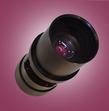
Specifying MWIR windows
When selecting optical materials, transmission is the top priority. To maximize system response, designers should select optical materials that have the highest transmission at the peak sensitivity of their chosen detector. Uncoated optical grade silicon features high transmission from 1.2um to 7um. Anti-reflective coatings can increase transmission to greater than 98%, which is ideal for MWIR applications.

Birefringence can degrade IR imaging performance, and silicon has an advantage here, too. Crystals with cubic crystalline structure exhibit no birefringence while non-cubic crystals will exhibit birefringence. Silicon is cubic in nature and will not exhibit birefringence.
Durability is an often overlooked aspect when specifying MWIR applications. Most IR transmissive materials are soft, brittle, and water soluble, which can be limiting depending on the application. Although transmission is the most important material property, MWIR applications can take advantage of silicon’s high environmental durability.
Weight sensitivity is also of particular concern in many IR imaging applications, especially if the device will be worn by the end user. The most popular IR materials, germanium and zinc selenide, are dense and add significant weight to the system. Silicon has a lower density (2.329g/cm3) making it ideal for weight-sensitive MWIR applications. Figure 1 provides a summary of properties for common IR materials.

Figure 1: Key IR Material attributes provided by Edmund Optics
Thermal stability is another key consideration in MWIR applications. The change in index with respect to temperature (dn/dT) of most IR materials is orders of magnitude higher than those of visible glasses. Silicon is thermally stable, characterized by a low dn/dT, particularly in respect to germanium.
Commercial applications of MWIR technology tend to be more cost-sensitive than defense applications. Due to its natural abundance in comparison to other IR materials, silicon is significantly cheaper, particularly as size increases. For example, a comparably-sized germanium window can be 2-3X more expensive.
The performance advantages of MWIR are driving more applications for MWIR lasers, which will, in turn, increase demand for high performance MWIR optics. Silicon’s optical properties — excellent transmission through the MWIR and lack of birefringence — combine with its durability, low density, thermal stability, and natural abundance to make it the material of choice for many MWIR applications.
Written by Katie Walker, Product Line Engineer at Edmund Optics