


Today, world-leading research and innovation hub in nanoelectronics and digital technologies imec, and ASML Holding N.V. (ASML), the technology and market leader in lithographic equipment, announce the next step in their extensive collaboration. Together, they will accelerate the adoption of EUV lithography for high-volume production, including the current latest available equipment for EUV (0.33 Numerical Aperture, NA). Moreover, they will explore the potential of the next-generation high-NA EUV lithography to enable printing of even smaller nanoscale devices advancing semiconductor scaling towards the post 3 nanometer Logic node. To this end, they will establish a joint high-NA EUV research lab.
Imec and ASML have been conducting joint research for almost thirty years. In 2014, they created a joint research center, the Advanced Patterning Center, to optimize lithography technology for advanced CMOS integration and to prepare the ecosystem to support advance patterning requirements. Now, they bring this cooperation to the next stage with the installation of ASML’s most advanced and high-volume production dedicated EUV scanner (NXE:3400B) in imec’s cleanroom. Utilizing imec’s infrastructure and advanced technology platforms, imec and ASML researchers and partner companies can pro-actively analyze and solve technical challenges such as defects, reliability and yield, and as such accelerate the EUV technology’s industrialization.
With a 250W light source, ASML’s newest EUV system throughput will be more than 125 wafers per hour, one of the industry’s most important requirements for high-volume production. The NXE:3400B will also be equipped with the latest alignment and leveling sensors, to enable optimal process control at this high throughput. This will facilitate the overlay matching of the NXE:3400B to that of the latest immersion scanner, NXT:2000i, that will also be installed in imec’s cleanroom in 2019. In addition, ASML and imec will expand the metrology capability with new ASML YieldStar optical metrology and ASML-HMI Multi-electron beam metrology equipment, allowing more accurate and faster evaluation of nanoscale structures.
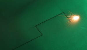
To continue on the leading edge of lithography development, a second component of the increasing collaboration is the foundation of a joint high-NA EUV research lab. In this lab, researchers from both organizations will experiment with the next generation of EUV lithography at higher NA. Systems with a higher NA project the EUV light onto the wafer under larger angles, improving resolution, and enabling printing of smaller features. More specifically, the new high-NA EUV system, EXE:5000, that will be installed in the joint research lab, will have an NA of 0.55 instead of 0.33 in current NXE:3400 EUV systems. Already now, the first joint scientific projects to facilitate the introduction of high-NA EUV, are ongoing. In the joint research lab, ASML and imec will perform research on the manufacturing of the most advanced nanoscale devices by high-NA EUV and assist the ecosystem of equipment and material suppliers to prepare for the introduction of high-NA EUV technology to the industry.