


Until very recently, there were only limited economic ways of recovering valuable materials from old and decommissioned electronic devices. After more than four years of research, the international EU project ADIR has now come up with a viable recycling concept based on the principles of urban mining and inverse manufacturing. Here, electronic devices are treated as repositories of recyclable materials, from which raw materials can be recovered once such devices have been withdrawn from circulation. In an automated procedure that has already been trialed in an industrial setting, a variety of laser processes are used to identify electronic components on printed circuit boards (PCBs) and then desolder and sort them.
ADIR (Next generation urban mining – automated disassembly, separation and recovery of valuable materials from electronic equipment) is a project that was funded by the EU’s Horizon 2020 program. Coordinated by the Fraunhofer Institute for Laser Technology ILT, it brought together a total of nine project partners from research and industry. The result was an entirely new recycling concept and a demonstrator that was then successfully tested on over 1000 cell phones and 800 printed circuit boards by the company Electrocycling GmbH. The trial showed that the ADIR demonstrator works in an industrial setting and that in some cases recovery rates are as high as 98 percent. Viewed strategically, the aim of the project is to lower the EU’s dependency on natural resources, reduce the need for costly imports of raw materials and demonstrate new technologies that will enable inverse manufacturing. The latter is considered as a key technology for a sustainable circular economy and is in line with the programmatic goals of the European New Green Deal.
Valuable materials in electronics
This is where the project partner Electrocycling GmbH entered the frame. The company is a certified recycler of decommissioned electrical appliances and electronic devices, based in Goslar, Lower Saxony (Germany). It processes 4000 metric tons of electrical appliances and electronic devices a month and therefore possesses the requisite industrial expertise. The company selected two main categories of material for processing with the ADIR demonstrator: cell phones along with the PCBs and batteries they contain, and the PCBs in computers and servers.

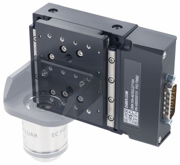
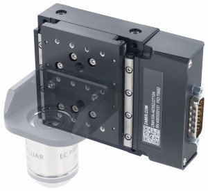
The ADIR demonstrator automatically identifies and analyzes components of electronic assemblies such as the printed circuit boards found in cell phones and computers. © Fraunhofer ILT, Aachen.
Valuable metals can be recycled from these components. These include tantalum from capacitors, neodymium from loudspeakers, tungsten from the counterweight in the vibration alarm, and gold, silver and platinum-group metals from the unbalance mass in the PCB components.
How does the ADIR process work?
The disassembly system is based on a smart combination of laser technology, robotics, vision systems and information technology. First of all, the cell phones are into the process line, where a robot picks them up and cuts open the casing. The electronics are then dismantled along with, if present, the battery, vibration alarm and loudspeaker. Just as with larger, manually loaded PCBs, these components are then analyzed and identified by means of a high-resolution imaging process, which compares them in shape and size with information logged in a database.
What takes place?
- Casing is cut open; battery and PCBs are removed; battery is disposed of safely
- PCBs are picked and placed
- High-resolution imaging (2D color and 3D) of the PCBs; image analysis of the geometry of target components and comparison with database
- Chemical analysis of the constituents of the components by means of a pulsed laser beam, which locally vaporizes a microscopic amount of the material and generates an emission spectrum of the element in question (laser-induced breakdown spectroscopy – LIBS); gained physical and chemical data of components are digitally logged in a database
- Desoldering of valuable electronic components from PCBs: scanning with a continuous infrared laser momentarily warms the respective solder pads and softens the solder; components are removed by means of a suction nozzle and then sorted into different fractions
- Other electronic assemblies are dismantled – and their components separated – by means of shock waves generated in a water-filled vessel by a rapid succession of electrical discharges; these components are then sorted
- Various multistage hydro- and pyrometallurgical processes are provided by H.C. Starck Tantalum and Niobium GmbH, Aurubis AG and the Åukasiewicz Research Network – Institute of Non-Ferrous Metals) for the recovery of so-called technology metals as a valuable stock of secondary raw materials
Various lasers are used for desoldering components and for LIBS; an additional laser is used for 3D imaging.
Tested for industrial use
Even the very best demonstrators are meaningless unless they meet industrial requirements. During 2019, the ADIR process underwent testing at the company Electrocycling GmbH and was validated for use in industry. These field trials demonstrated, for example, how a combination of various processes can be used to remove substantial numbers of small capacitors from PCBs in order to recover the valuable metal tantalum from them. In this case, the recovery rate for tantalum was between 96 and 98%.

Successful recycling: in the ADIR project coordinated by Fraunhofer ILT, disassembly of around 1000 cell phones and over 800 printed circuits boards produced several kilograms of components from which valuable materials could then be recovered. © Fraunhofer ILT, Aachen.
The precompetitive project is now complete. With the demonstrator, the ADIR team has been able to prove the industrial viability of the new method. Based on the project findings, part of the process chain can now be realized. This includes inspection of the PCBs as well as desoldering and removal of valuable target components. Meanwhile, there is still scope for improvement in areas such as automation, which should help speed up the process. Initial experience with automated processes to cut open and disassemble cell phones has already been gathered and collated in a database. In the future, this data can be used by employees to train a recycling unit to handle new cell phone models.
The process has sparked interest from industry, with several implementation partners already secured, and others now being sought. This new concept not only promises a more efficient use of raw materials but will also reduce European dependence on imports of raw materials from around the world and create new opportunities to introduce the kind of inverse manufacturing technologies that are required to establish closed material cycles.
ADIR (Next generation urban mining – automated disassembly, separation and recovery of valuable materials from electronic equipment) was conducted as part of the EU’s Horizon 2020 program. The ADIR project partners are:
- Fraunhofer Institute for Laser Technology ILT, Aachen, Germany (project coordination)
- Aurubis AG, Hamburg, Germany
- Electrocycling GmbH, Goslar, Germany
- Fraunhofer Institute for Factory Operation and Automation IFF, Magdeburg, Germany
- H.C. Starck Tantalum and Niobium GmbH, Goslar, Germany
- Institute of Non-Ferrous Metals, Gliwice, Poland
- Laser Analytical Systems & Automation GmbH, Aachen, Germany
- OSAI A.S. S.p.A., Parella, Italy
- Tre Tau Engineering s.r.l., Turin, Italy
Written by Dr. Cord Fricke-Begemann, group manager for materials analysis, Fraunhofer ILT
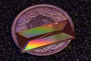
Caption for photo at top: The new recycling concept focuses, in particular, on the elements tantalum, neodymium, tungsten and gallium, which are to be found in virtually all modern electronics. © Fraunhofer ILT, Aachen.