


Historically, ‘latency’ describes the time interval between stimulation and response, cause and effect. Contemporary use has considerably widened the terminology to include functional aspects of architecture, capital markets, bandwidth, robotics and more. In this article we use the term in an engineering/commercial sense and more particularly in regards to improving dynamic efficiencies in the microelectronic packaging process—from concept to full-scale commercial manufacturing. The most critical points of low latency engagement are those adopted in the initial stages. These tend to take on a life of their own and adopted thoroughly enough have an exponentially growing impact—and value—down the development chain. By analogy, the more accurate your final coordinates the less often you have to stop and reorient.
Low latency manufacturing is not necessarily about approaches to efficiency per se, but (i) where it takes place, (ii) the people and (iii) the level of customer connectivity.
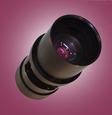
In the lidar ecosystem, additional pressure comes not only from rapidly growing markets but application diversification; mapping to wind, to automotive, to oceanic topography to robotics. Indeed, the latter is quickly becoming an ecosystem in itself. While the fundamental lidar concept is the same in each case, differing end-uses can have a big impact on packaging approach, materials used, size, complexities and integration levels. Finally, as many readers will be aware, there is the medium-term push to fully integrate laser and sensor, potentially radically reducing the number of discreet components. These pressures are all amplified by additional critical factors ranging from the premium placed on innovation to the impact of hyper-intense competition. In short these all require a packaging manufacturing culture that is acutely ‘green and lean’, agile and efficient.
Application of best-practice low latency manufacturing
A best practice low latency approach begins with a three-fold foundation:
- Establish a time-framework with the customer for the project. This tightens up a series of crucial technical parameters. It may seem obvious, but as a principle it is more poorly executed than not.
- Involve the entire team in the project. Bringing together motion control, tooling, software, hardware experts and others, with non-engineer commercial oversight, means all the core competences are together in the same room for strategy and implementation simultaneously embedding a high-level of commercial cognisance
- Optimise the equipment/software for the task at hand.
In practical terms these are then combined to produce the metrics by which the efficiency of low latency manufacturing protocols are judged:
- High yields secured through the efficient use of time, materials and personnel.
- Optimum return on investment secured through high net throughput.
- Minimise labour training, maximise labour efficiency and minimise the impact of labour turnover for ease/security of manufacturing.
Short-comings in each project are fed back into the team for immediate changes and always documented for future improvements.
Four pillars of low latency manufacturing in lidar packaging
These practices can be formerly separated into the ‘Four Pillars of Low Latency Manufacturing’ identified below:
- Continuous collaborative learning.
- Proof of concept and strategic implementation of critical design elements.
- Prototype development.
- Product and process maturation.
Having said that, and as the illustration below indicates, once put into practice these conceptual pillars quickly dissipate into a dynamic entity. Order needs to be followed but when technical activity starts the wider principles of ‘lean and green’ and commercial cognisance direct the whole.

Lidar specific packaging projects start out with expert-to-expert engagement following a structured but fluid two-way learning process. As implied, pre-determined parameters have been set to ensure relevance and timeliness. This allows sharp focus on customer’s context and the subsequent and critical elements in the technical and commercial needs behind the desired lidar product to be swiftly implemented. Best practice means that the team are able to quickly cut through a number of alternatives based on experience to meet customer’s actual needs.
From here on in a more technical and focused collaboration begins by exploring the nuances of the desired optical coupling for the specific assembly against fundamentals such as active or passive alignment. Thereafter potential adhesive selections are weighed against the back-drop of such constraints as thermal conductivity.
In the example of lidar these include the critical elements of transceiver and receiver assemblies, creating test features for PICs, short loop wafer processing, scaled down chips, etc., for testing/proving purposes. It is also important to create sufficient but not fully functional and therefore inexpensive but effective design test pieces. This permits many variations and independent testing. The latter can be especially beneficial by excluding sub-par or tangential practices early on.
Getting up to speed in the prototype process can be one of the most critical times for learning. The value of generic cost effective tooling to undertake small volume builds, varying materials, parameters and processes within tightly defined and pre-verified limits is self-evident. Pre-verification is also important in securing accurate metrics in turn minimising cost and use of time. An extraordinary amount can be learned in the first 10-100 units and having a ‘green and lean’ philosophy enables making quick revisions across a large range of areas. The whole process yields vital data that vendors often fail to share with their customers. Once in a while this leads to the entire redraft of the project or even abandoning it altogether. Yet even a ’failure’ in the commercial value can vindicate a low latency process.
Transitioning toward full-scale low latency manufacturing production
Most of the time, however, a successful process is identified and mapped out for movement towards full-scale commercial production. Often that means transferring low latency manufacturing process to the customer’s production facilities. When low latency practices are robustly developed using the four pillars of manufacturing, this secures a robust and mature production process from day one. Immediate benefits include yield, optimum automation, proven and sustainable hardware options, proven and sustainable software options, proven metrics and often swift root cause analysis. In short, low latency manufacturing reduces the most complex processes into their simplest solution form at whatever point and however many parts of the process they are applied.
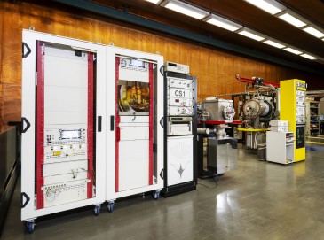
Palomar Innovation Centres represent ‘a bridge of ability’ that spans all the way from the original idea to full commercialised production. What has given Palomar a ‘head-start’ in the ‘green and lean’ advantage is our long history of collaboration in packaging development across a spectrum of core technologies; 40 years of experience in VCSELs/light engines, packaging RF GaN and other processes requiring similar competences.
Our low latency manufacturing strategy brings together core areas of design, process approach and manufacturing. This in turn provides feedback, iteration and timely action. The result is not only a better product more efficiently manufactured but one with higher returns on capital outlay.
Looking ahead, m2m (machine to machine communication) deep learning, XR and AI are all going to have an extraordinary impact on the low latency aspects of manufacturing. Critical elements from the fundamental idea to packaging design to process, will increasingly incorporate these elements, and most especially diagnostics of issues that arise on the way together with suggested solutions.
Notwithstanding, human insight, experience, intuition, commercial cognisance and the synergies between skill-sets and competence will always be at the heart of the design and manufacturing process.
Written by Dr. Anthony O’Sullivan is Palomar Technologies’ Strategic Market Analyst, based in Shrewsbury, the UK. Nick Evans is the Sr. Process Engineer at the Carlsbad Innovation Center, California, USA.