


Many image sensor manufacturers have traditionally supported what is known as the Low-Voltage Differential Signalling (LVDS) interface in their products. This interface, which specifies the electrical characteristics of a differential, serial communications protocol, enables camera developers to route the data output from a CMOS image sensor into an FPGA, where a variety of operations can be performed.
According to Mirko Benz, a Product Manager at Baumer Optronic, the differential signalling approach used by the LVDS interface requires the use of two complementary signals that work as a pair or a channel. Each pair of such signals enables data to be transferred from the image sensor to the FPGA at rates at about 600Mbit/sec.
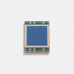
While earlier image sensors supported 8, 16, and 32 pairs, the demand for increased speed now means that many larger high speed imagers support 64 LVDS pairs, allowing them to transfer data to the FPGA at an aggregate rate of 4GByte/sec. Of course, with such wider interfaces, the design of a camera becomes more complex; a fact that is reflected in the price of the camera itself.
Scalable Low Voltage Signalling with an Embedded Clock
According to Damian Nesbitt, the Director of Platform Software at Point Grey, however, next generation sensors from Sony will eschew the use of the older LVDS interface technology in favor of a new standard called Scalable Low Voltage Signalling with an Embedded Clock (SLVS-EC), which will soon debut on their next generation of image sensors aimed at the industrial camera manufacturer.
At VISION 2016 in Stuttgart earlier this month, Nesbitt said that the high pin count of sensors needed to support the transfer of high speed image data over the LVDS interface leads to the need to use an FPGA with an equally large pin count. By using the new Sony SLVS-EC interface, however, it is possible to design a high-speed interface with a lower pin count. As a result, the cost of building cameras with high resolution and high data rates will be lower, although imaging sensors that support the new interface are not expected to be widely available until the third quarter of 2017.
The Scalable Low-Voltage Signalling (SLVS) technique is based on a point-to-point signalling method that has evolved from the traditional LVDS standard. As many design engineers are aware, LVDS channels have a low susceptibility to noise because sources of noise add the same amount of common-mode voltage to both lines in a signal pair. As its name would imply, SLVS also has a low susceptibility to noise, but because the specification calls for smaller voltage swings and a lower common-mode voltage, lower power drive circuitry can be used to drive the interface.
According to Christopher Baldwin, the Manager of Technical Services at Framos the notable feature of the new Sony interface is that it makes use of an embedded clock. In the earlier LVDS design, separate clock sources are used to enable the FPGA to accurately recover synchronized data from the imager.
In the SLVS-EC design, the clock signal is embedded in the data from the imager and recovered by dedicated circuitry on the FPGA. Hence the data can be transmitted at much higher data rates and over much further distances.
Supporting the new standard
More specifically, each of the channels on the SLVS-EC interface can support effective data rates of up to 2.304Gbit/sec. The result is that a sensor that supports the new standard will be able to transfer data over eight lanes at a data rate of 1.84GBytes/sec (80% of full bandwidth due to 8b10b encoding), comparable to an LVDS system that requires thirty-two lanes to match almost the same data transfer rate. The longer signal path lengths that can be achieved, on the other hand, will be invaluable to designers of embedded systems who wish to develop camera-based systems where the FPGA circuitry is located some distance from the imager.
Baumer Optronic, Point Grey and Framos all indicated that they would be debuting high performance cameras based on the interface in the 2017-2018 timeframe as samples of Sony imagers that support it become more widely available. However, one Japanese company – Macnica and French electronics distributor – ATD Electronique had already received an early technical sample of a Sony SLVS-EC imager and were demonstrating a system based around it at the Vision 2016 show.

At VISION 2016 show, Macnica and French electronics distributor ATD Electronique were demonstrating a system based around a Sony SLVS-EC imager. The system took the data from the sensor and transferred it over a four lane SLVS-EC interface to an Altera FPGA based board that used a combination of Macnica’s own SLVS-EC Rx IP and Altera’s Transceiver IP to output RAW still image data to a PC via USB 3.0, as well as live video images to an HD monitor over an HDMI link.
The system in question took the data output from the Sony image sensor and transferred it over a four lane SLVS-EC interface to an Altera FPGA- based board that used a combination of Macnica’s own SLVS-EC Rx IP and Altera’s Transceiver IP to output RAW still image data to a PC via USB 3.0, as well as live video images to an HD monitor over an HDMI link.
Undoubtedly, the new Sony interface will become one of the new de-facto standards used to interface cameras to FPGA over the coming years. There are already some SLVS-EC Sony sensors available for use in use in consumer applications, and at VISION 2018, engineers can expect to see cameras based on Sony global shutter sensors with the new interface. In the meantime, the LVDS interface will still be widely employed in many cameras that target the machine vision market.
At VISION 2016, for example, Baumer Optronic was previewing a camera based around the LVDS interface, which will become available in the third quarter of next year. The camera, which is based on a 12Mpixel CMOSIS global shutter sensor transfers data from the sensor via 64 LVDS lanes into an FPGA at 4GBytes/sec. A 2GByte image memory buffer is used to buffer the data, which is then transferred over a 10GigE interface at a slower speed of 1GByte/sec.
Not the only interface in town
It must be stated, however, that LVDS is not the only standard interface in town. Michael DeLuca, the Go To Market Manager at image sensor manufacturer ON Semiconductor,notes that his company produces devices that use not only LVDS, but also HiSPi (a different low-voltage interface), MIPI and some with parallel CMOS outputs. In fact, several of the company’s devices support more than one of these to help simplify camera design depending on the specifics of the end application being considered.
Written by Dave Wilson. Senior Editor, Novus Light Technologies Today