


Perovskites are mainly known for what they bring to the field of solar cells. Researchers from IMO-IMOMEC, an associated laboratory of imec at the University of Hasselt, and colleagues from KU Leuven, UGent and UAntwerpen, are tuning perovskites also for other applications. It is the combination of good opto-electronic properties with low material and manufacturing costs that makes perovskites a promising material for any application in which light absorption, emission and detection is involved.
Together with several leading companies, the team will explore what perovskites can do for X-ray and lasers, as well as for solar cells. For X-ray detectors, the use of perovskites could lead to improved image quality, which can be translated into significantly lower exposure levels for medical or security screening of humans. For lasers, the new material development aims at increasing the material gain coefficient to 1000cm-1 or more, resulting in more cost-effective projectors with better resolution. For solar cells, perovskite materials with enhanced moisture and thermal stability will be developed.
IMO-IMOMEC is an associated laboratory of imec at the University of Hasselt that specializes in material research. Along with Dirk Vanderzande from the University of Hasselt, we started our research on perovskite materials in October 2015. One year earlier, imec launched its perovskite solar cell research. Imec and IMO-IMOMEC work in a complementary way, with the same goal: where imec strives to make better perovskite solar cells by changing interfaces and architectures, our group contributes on the chemistry aspects of the materials. Bringing both tracks together (imec using our most promising novel materials with their new engineering tricks) is the key to success in perovskite solar cell development.
Looking beyond solar cells
With the new SBO project PROCEED, funded by FWO, the IMO-IMOMEC research group wants to strengthen its perovskite research for solar cells and broaden the application field of the promising material toward other industries. If we could find new applications beside solar cells for the material, this could boost the interest of industry to commercialize and further mature the material. We believe that perovskites are very promising materials for many light-emission and light-detection applications. In the new project, we will use our expertise on perovskite for its use in conversion, emission and detection of light.
The holy grail of perovskites
Perovskite is a family of materials that has been known for some time because of its intriguing physical properties. It has been studied e.g., as a piezoelectric material, as superconductor, or to catalyse chemical processes.
A key characteristic of hybrid perovskites is its astonishing versatility, both in terms of composition, dimension and morphology. First of all, the composition of metal halide perovskites can vary: if you take the generic chemical formula ‘APbX3’, X can either be chlorine, bromine or iodine, whereas A stands for different possible cations such as methylammonium, formamidimium or cesium. Second, thanks to this compositional freedom, material scientists can create hybrid perovskites with different dimensionality, going from regular 3D materials to materials that have an intrinsic (quasi-)2D or even 0D structure. And thirdly, perovskites can be synthesized with many different morphologies, such as thin films, single crystals, microcrystals or nanocrystals.
The main challenge
The main challenge in hybrid perovskite research today is the lack of long-term stability.

Hybrid perovskites are a very versatile material that can be tuned for different applications. (Please note that the terms 3D and 2D here relate to the structural motifs and not to the actual dimensions of the materials.)
Perovskites for Solar Cells: Toward 2D perovskites for more stability
Crystalline silicon-based technologies are currently dominating the PV market. Typical commercial module efficiencies are about 17-18%, with a record commercial product efficiency of 22.8% and the theoretical limit being over 29%. One way to reach a higher conversion efficiency, is by stacking different semiconductor materials, each with their specific bandgap. Each layer is suited for a specific part of the light spectrum and in this way higher efficiencies can be reached.
Tandem solar cells combining silicon and perovskite solar cells could be the answer to solar cells exhibiting both high efficiency and low costs. The low cost of a perovskite-based solar cell comes from the fact that the material itself is not expensive, only thin films are used and the process technology via printing/coating is relatively simple and doesn’t require any expensive equipment.
Ideal for BIPV
Moreover, because of their semi-transparency, their light weight and the possibility to produce them on flexible substrates, they are ideal candidates for BIPV (building integrated photovoltaics). The ease of processing allows for customization in dimensions as well as in design (color, transparency), an important asset to convince architects of using more solar technology into their buildings. And, because the efficiency decreases less at higher temperatures (as compared to crystalline silicon solar cells) they could be integrated in insulating glazing. Next to that, perovskite solar cells could be integrated into roof, architectural glass, walls, tiles, facades and shingles. In these cases, the orientation of the solar cells is less of an issue because of the better response to diffuse light conditions than silicon solar cells.
")
Vision of perovskite-based solar cells being integrated in the windows of a building.
It’s the limited stability that holds back any practical implementation of the demonstrated high efficiency perovskite solar cells. The material scientists at IMO-IMOMEC are tackling this by trying to make more robust hybrid perovskites by tuning the composition to obtain an improved moisture-resistivity.
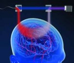
Perovskites for X-ray: thick and large layers are key
For many years, the most common technology for X-ray imaging was based on photographic film. In the film-based detector X-rays were converted to light by intensifying screens and the light created a latent image on the film that became visible after development. Today, this process has been replaced by digital technology: the X-ray image is detected with a flat-panel detector. In indirect type digital radiography (DR) detectors, the X-ray photons are converted into light by a scintillator, just like in a film-based detector. This light is then converted into charges in a photodiode which are collected on pixel electrodes. Upon image read-out the charges are converted into electronic current via the TFT based detection system. The signal is turned into electronic data which in turn is transformed into a high-quality digital image. For direct type DR detectors, the X-ray quanta are directly converted into photo-charges which are in a similar way converted in to a high-quality digital image. The optical intermediate step in indirect type DR detectors causes some blurring because of light scattering and reflection in the scintillator layer and in the interfaces, leading to unsharpness in the images.
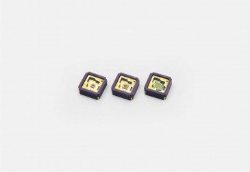
Amorphous selenium (a-Se) is most often used as direct conversion material in digital radiography. For high energy photons, the attenuation in the a-Se layer is however very low, limiting the use of the a-Se detectors to mammography applications. In recent years, perovskite materials based on high Z elements have been tested for X-ray detection in order to make high image quality detectors for general radiography applications, allowing reduced radiation dosage for patients. As perovskite layers can be applied by low cost methods at low temperature even on flexible substrates, this new approach would make a low cost, low weight, robust, large format and potentially flexible X-ray detector feasible. This would enable the broader use of X-ray scanners for health applications (human and veterinary), for industrial use and for security. Industrial detectors can e.g. be used for non-destructive quality control in industrial branches such as automotive, aerospace, defense and power generation. Also, in security domains, X-ray is a growing market because of the globalized traffic and trade and the growing need to scan people and cargos at the border checkpoints.
As a starting point, perovskites for the commercial market were used. However, other characteristics are required: X-ray detectors on one hand need very thick layers and materials with a high atomic number. The latter to realize a high X-ray attenuation. As a consequence, a higher voltage across the layer is required to efficiently collect the generated photo-charges.
Within the project PROCEED, the partners are researching how to realize a thick layer of microcrystal perovskites on a large surface (43 cm x 43 cm), and this at an acceptable cost. This requires innovative processing approaches. And because we are working with thick layers of several hundreds of micrometers, we try to develop also alternative, Pb-free perovskites.
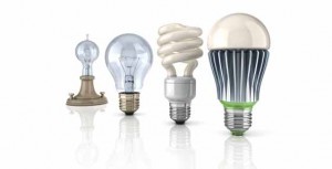
Perovskites for light projectors: nanocrystals to ‘pump up’ the lasers
Light sources for light projectors need to reproduce as many visible colors as possible, with high brightness and minimal power consumption. Lasers are ideal candidates for this and have a much better performance and lifetime as compared to the traditional high-pressure lamps (in the case of projectors).
Current laser projection systems use a focused blue laser to pump a luminescent material such as YAG:Ce to generate the red, green and blue primary colors from a point source. This approach has a limited optical efficiency since the pumped spot acts as a non-directional Lambertian emitter and color filtering is needed to generate the red and green primary colors. Alternatively, laser projection systems rely on 3 different lasers to generate red, green and blue, a costly approach that offers limited options to eliminate intrinsic problems of laser projection, such as speckle.
It would be possible to combine a commercial blue laser – the most performing of the red/green/blue set – with low-cost, optically pumped red and green amplified spontaneous emission sources or lasers. Perovskite nanocrystals could be used as green or red gain material and this approach would reduce the complexity and cost (a large cost reduction of 30-40% for the projector light source is expected) of high-end laser projectors. The tunable bandgap and high optical gain of perovskites are important in this context.
Perovskites promise lower cost, higher performance
Because perovskites are so versatile, they could be used for many applications. Until now, mainly solar cells were on the agenda of perovskite material developers and researchers. And although there are still some major issues with perovskite-based solar cells, it is worthwhile to explore and tune perovskite chemical structures also for other applications. IMO-IMOMEC, an associated laboratory of imec at UHasselt, is doing this. In Proceed, the consortium is developing novel 3D/2D perovskite structures to tackle the stability issue in solar cells but also focusing on fabricating thick perovskite films with large dimensions for X-ray applications, and perovskite nanocrystals as gain material for lasers for light projectors. In all these cases, the use of perovskites promises a lower cost and and better performance.
PROCEED is an SBO project funded by FWO (S002019N) bringing together partners from 4 Flemish university’s and 1 research center.
Written by Laurence Lutsen, Strategic Research Manager and Project Manager at IMO-IMOMEC associated laboratory of imec in Hasselt, Belgium.