


Rofin reports that laser systems can enhance cell efficiency above 20% for mono-crystalline and 18% for multi-crystalline cells and modules.
Rofin systems are able to process C-Si solar cells in many ways: PERC processing, selective emitter, laser fired contacts, metal wrap through, marking and cutting; with PERC and selective emitter being the trends of today.
A highest efficiency gain of up to 1% (absolute) can be realized on standard solar cells with a PERC cell design architecture. Due to continued application research and cooperation with material suppliers, Rofin can also recommend suitable aluminum pastes for the PERC process. This is perfectly complemented by a selective emitter structure via laser doping of PSG (Phosphor Silicate Glass) into the silicon surface, adding another 0.3% efficiency gain. Laser doping widths of less than 200 micron significantly enlarge the total area with reduced recombination and better blue light response.
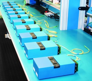
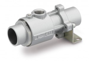
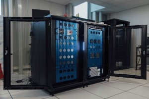
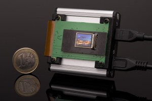
Rofin successfully introduced fully integrated laser manufacturing systems for rear side passivation, selective emitter and MWT processes to high volume c-Si cell manufacturers over the last 3 years. Recent orders also included new installations of Dual Line c-Si machines specifically for PERC cell processes. According to Rofin, the core of the machine is a high-precision granite base to support the laser optics and rapid wafer handling units.
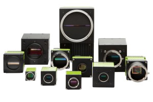
Features include a standardized HMI software, gentle wafer handling for highest yields, and a powerful PLC system allowing a throughput range of 1800 – 3600 wafers per hour. The system can be placed in-line with other processing machines or configured with stack and/or cassette handling systems for batch type operation. The whole range of Rofin laser sources in 1064, 532 and 355 nm wavelengths and various pulse length regimes from continuous wave to femtosecond are available addressing high cell efficiency processes.
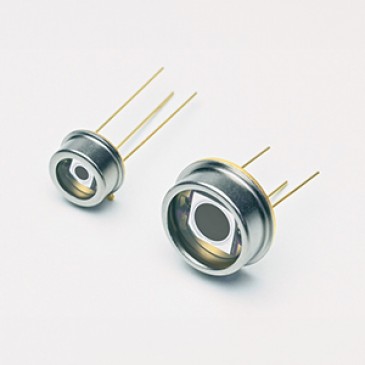
Ultrashort pulse lasers, like the StarPico and StarFemto FX, can also be used to enhance PV manufacturing.
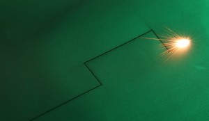
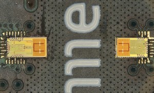
The patterning of CI(G)S thin-film cells relies on high quality P1, P2, and P3 scribes. Better quality scribes will immediately lead to significantly smaller dead zones and higher module efficiency. Each scribing process addresses a different thin film (metallic back contact, CIGS absorber material, TCO) and has its own challenges. However, picosecond lasers offer superior processing quality for all three scribes, namely a sharper ablation profile, less molten CIGS and complete avoidance of layer separation and micro cracks.
Regarding crystalline solar cell manufacturing, ultrashort pulse lasers have already shown their potential for structuring SiO2 and SiN layers and edge isolation. Current ablation processes on solar cells are mainly based on indirect ablation. The laser energy is transmitted through the transparent dielectric layer and absorbed in the topmost layers of silicon. To shift ablation closer to the direct absorption, laser pulses must be as short as possible to maximize pulse peak power and minimize heat impact to the layer underneath. Recent studies, performed by ISC - Konstanz with a Rofin StarFemto FX laser source, showed that laser ablation with negligible damage of the silicon underneath the ablated dielectric layer can be performed.