First introduced in 2008 as the result of a joint development between Andor Technology, Fairchild Imaging (part of BAE Systems), and PCO, sCMOS cameras have now become a vital tool in the arsenal of scientists working in the field of bio-imaging who need to capture images to determine how living cells and tissues function.
Prior to the introduction of these new cameras, scientists were limited to using either CCD or EMCCD cameras, both of which had their own set of technical limitations. And although these cameras are still widely used, there is no doubt that the inherent advantages of sCMOS cameras have now made them a viable contender for many scientific applications where their counterparts were previously employed.
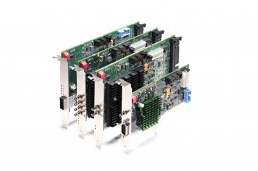
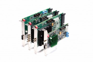
Today, both monochrome and RGB sCMOS image sensors are available from manufacturers such as BAE Fairchild and GPixel. Notably, many camera manufacturers such as Andor, PCO, Photometrics, Princeton Instruments, Hamamatsu, Thorlabs and Tucsen, have taken advantage of the new sensors, building them into a variety of both monochrome and RGB sCMOS cameras with a variety of standard industry interfaces.
Comparing differences
Comparing the differences between cameras based on CCD and EMCCD imagers and those based on new sCMOS designs in terms of certain characteristics such as resolution, pixel pitch, frame rate, readout noise, dynamic range and quantum efficiency is relatively straightforward.
Sensors with smaller pixel pitch sizes, for example, will have higher limiting resolutions while sensors with larger pixels will have lower limiting resolutions. The higher the frame rate, the greater the number of individual images that can be captured per second -- important when considering the fact that the frame rate and the exposure time of each frame, are directly correlated.
Quantum efficiency – the real parameter defining sensitivity -- is defined as the number of electron-hole pairs created and successfully read out by an imager for each incoming photon. High quantum efficiency sensors are especially important in low-light imaging applications such as fluorescence microscopy, where emission photon wavelengths are often in the 375-550 nanometer range and have a relatively high absorption coefficient in silicon.
The dynamic range of the sensor is equally as important, as it represents the ability of a system to capture the brightest and darkest portions of the image and the number of variations between. It is defined as the ratio between the full well capacity and the noise floor, which itself can contain sensor readout noise, camera processing noise and dark current shot noise. Today, it is not uncommon for contemporary sensors to sport dynamic ranges of over 30,000:1.
According to Dr. Ruediger Bader, the Sales Manager at Photon Lines, however, it is the noise characteristics of the sensor that are possibly the most important criteria when comparing imaging systems, because they determine the detection limit of the system. The higher the signal-to-noise ratio, the better a system is able to resolve objects under low light conditions.
“In general, it is always better to have a high signal-to-noise ratio. But the only way to increase the maximum signal to noise ratio is to increase the full well capacity of the imager. If the signal is just photon noise limited, the only way to improve it is to collect more photons. In the extreme, this means that a single photodiode, as large as an image sensor, would have the largest full well capacity and the best possible signal to noise ratio, but unfortunately no information,” said Dr. Gerhard Holst, the Head of Science and Research at PCO.
Different types of noise - such as dark current noise, readout noise, amplification noise and shot noise, may be generated by each sensor and in some cases, the type of noise generated, specifically dark current noise, is temperature and exposure time dependent. However, these different types of noise do have a profound impact on the characteristics of the cameras developed around the sensors.
CCD, the de facto standard
Since they were introduced, charge coupled devices (CCDs) became the de facto standard imager for many scientific applications. Back-illuminated CCDs boast a high quantum efficiency of 90%, which is achieved by focusing an image on the backside of the CCD image sensor. However, because the charge from each pixel in the sensor is always transferred through a common readout, the performance of CCDs has been limited by the readout noise created at the output amplifier of the imager. Notwithstanding, this has been the advantage of CCDs, because it is easier to optimize the noise behavior of one output amplifier instead of the thousands of output amplifiers in CMOS image sensors. However, to reduce this noise, the readout speed of the sensor, and hence that of the camera, has to be reduced to around a few seconds to effectively read an image from the device.
EMCCD sensors
Electron multiplying CCD (EMCCD) sensors -- introduced by e2V and Texas Instruments -- were developed to address this issue. In these devices, the signal must pass through an additional gain register before it is read out of the CCD array. Because the signal is amplified prior to readout, the signal becomes larger while the readout noise stays the same, giving a better signal to noise ratio. This also removes the restriction of having to reduce the speed of readout from the device.
However, the amplification mechanism required to reduce the effective read noise does itself introduce an additional noise source called multiplicative noise. However, the addition of this multiplicative noise is offset by the reduction in the readout noise which becomes dominant at specific frame rates -- which in EMCCDs are still low compared to readout rates of CMOS or sCMOS sensors. Hence the effect of amplifying the signal effectively eliminates the contribution of the read noise to the resolution limit of the imager.
“Before the advent of sCMOS imagers, a CMOS image sensor had thousands of amplifiers and they were not all noise optimized, but simply fast, while CCDs and EMCCDs had nicely optimized output amplifiers and A/D converters. If you compared a good Sony or Kodak CCD, they had readout noise values down to 8 – 5 e-, while CMOS image sensors -- even good ones -- had readout noise values of 13 e- and above,” said Dr. Holst.
Development of the sCMOS
In an effort to resolve that issue, the Andor, BAE Systems and PCO engineers co-developed the sCMOS, or scientific CMOS, sensor. The new type of CMOS sensor sports extremely low read noise to preserve small signal levels, an ability to collect and convert light with a high efficiency and is also able to operate at high speed and with a wide dynamic range. According to PCO’s Dr. Holst, the ability of the sCMOS sensor to do so was achieved by a clever architecture that employed dual amplifiers and an 11-bit readout. Because two 11-bit A/D converters can be read out slowly, this reduces the noise contribution as opposed to the noise obtained when reading out faster from a single 16-bit A/D converter. This enabled sCMOS sensors to achieve noise values of 1.1 e-. The high frame rate was reached by using a split readout scheme in which the sCMOS imager was split into two halves, which enabled the total frame rate to be doubled.
Early sCMOS sensors featured a microlens array to focus the incoming light away from the transistors on the face of the device and onto the exposed silicon, enhancing the quantum efficiency. Today, however, some newer sCMOS sensors are back illuminated, and have enabled camera developers to deliver an even greater quantum efficiency.

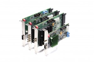
Kuro, from Princeton Instruments, is a back-illuminated scientific CMOS (sCMOS) camera system with up to 2048 x 2048 pixel resolution and low read noise.
Until now, this back illuminated technology was almost exclusively the domain of CCD-based camera systems, which are now unable to match the performance characteristics of sCMOS cameras.

Unlike front-illuminated sCMOS cameras, back illuminated sensors do not use microlenses to recapture light from a masked area of the pixel. On the other hand, back illuminated sensors can suffer from higher dark currents and lower Mean Time to Failure (MTF).

Enabled by PCO’s new back illuminated sensor, the PCO.panda reaches a quantum efficiency of up to 95%. This makes the camera perfectly suited for low light conditions without the need for active cooling.
According to Photon Line’s Dr. Bader, when choosing a sCMOS camera for any application, the optics used in the system must be matched to the size of the pixel in the imager. While a greater number of pixels in an imager can provide a higher resolution image, of equal importance is the choice of the lens. Hence the sensor pixel size of the imager becomes a decisive factor in selecting the correct lens for a particular application.
Many modern megapixel cameras use small sensor sizes to reduce costs. However, these need higher quality and more expensive optics in order to resolve light down to the smaller pixels. And usually smaller pixels have meant lower fullwell capacity, which in turn reduces the dynamic range. In certain case, it may be more advantageous to choose a more expensive megapixel camera with larger pixels that requires less demanding optics.
Certain sCMOS cameras sport pixel sizes of 11um x 11um. This is a perfect solution for scientists who wish to capture images of samples at 100um resolution using a 100x objective lens. When sCMOS imagers with pixel sizes of 6.5um x 6.5 um entered the market, scientists then had the opportunity to image with a 60X objective lens without losing spatial information, because the 6.5 6.5um x 6.5 um imager is better matched to the 60x lens than the 100X. It also enabled scientists to “bin” (or sum) neighborhood pixels on the imager to create a 30 micron by 30 micron pixel, thereby enabling the magnification to be increased to 100x.
Rolling or global shutter mode
One final consideration when looking to choose one of the many new sCMOS cameras that are now on the market is to determine if it supports a rolling or global shutter mode -- or both. Rolling shutter essentially means that different lines of the array are exposed at different times, while in global shutter mode all pixels of the imaging array are exposed simultaneously. While the lowest readout noise and fastest frame rates are available from rolling shutter mode, for some particular applications, for example where it is required that different regions of the image maintain temporal correlation, global shutter will be viewed as a necessity.
Written by Dave Wilson, Senior Editor, Novus Light Technologies Today