Silicon photonics has attracted an immense amount of attention lately because of its potential to offer a low-cost, high-density, energy efficient, reliable and scalable platform for the integration of photonics, electronics and micro-optics using mature CMOS fabrication technologies. Silicon photonics technology is expected to benefit a wide range of applications including, but not limited to, telecom, datacom, sensors, and instrumentation. However, the varied nature of the devices on a photonic chip poses unique challenges for the design and performance modeling of silicon photonic circuits. This article focuses on the design and performance of silicon photonic modulators, mainly the travelling-wave Mach-Zehnder modulator (TW-MZM). We begin with the challenges involved in modeling the TW-MZM device. Later, we estimate the impact of foundry processes on the performance of a transmitter chip that uses the TW-MZM. This case study not only helps photonic foundries estimate the yield, but also helps chip designers understand performance bounds due to the tolerances in the fabrication process. The modeling tools used for this case study are RSoft OptSim Circuit, RSoft FemSIM , and RSoft Multi-Physics Utility -- all from Synopsys.
Travelling-Wave Mach-Zehnder Modulator (TW-MZM)
Photonic modulators are an essential element in optical transmitters. Their main function is to modulate light with data so that the information can be transported over optical fibers. Transmitter performance depends upon modulator parameters such as insertion loss (the less the better), extinction ratio (the higher the better) and bandwidth (the larger the bandwidth, the faster the data rates it can support). The performance of silicon modulators is also sensitive to operating temperature. One of the bottlenecks in current high-speed fiber-optic systems is lack of efficient modulators that can support data rates of 40 Gbps and above. To achieve wider bandwidths, travelling-wave electrodes are required in the MZM design. For efficiency, speed and power consumption reasons, these electrodes require impedance and velocity matching, as well as low loss. The next section examines modulator performance when wafer-to-wafer (WTW) and run-to-run (RTR) variations in the silicon photonic foundry processes impact impedance matching.
TW-MZM device model
The velocity mismatch between the optical wave and the radio frequency (RF) wave can limit the performance of the TW-MZM. Both the optical and RF modes, as well as their dispersions, were calculated rigorously at the device level using RSoft FemSIM, a mode solver based on the finite-element method. For a structure similar to the one reported in reference [4], the calculated optical mode at wavelength of 1550nm and RF modes at frequency of 10GHz are shown in Figures 1 and 2, respectively.

Figure 1: Ex and Ey profiles as well as the vector plot of the calculated optical mode

Figure 2: Ex and Ey profiles as well as the vector plot of the calculated RF mode
The calculated mode shape and effective indices are different. As a result, their propagation speeds are also different (2.566727 and 2.253828, respectively), which is the main limiting factor for the modulation speed of this TW-MZM.
Because of the electro-optical effect, the applied RF signal changes the electron-hole density around the PN junction inside the core of the optical waveguide. Consequently, carrier density change causes a refractive index change and affects the effective index of the optical mode. The electro-optical effect was simulated in the RSoft Multi-Physics Utility. The calculated effective index of the optical mode at different bias voltage is shown in Figure 3.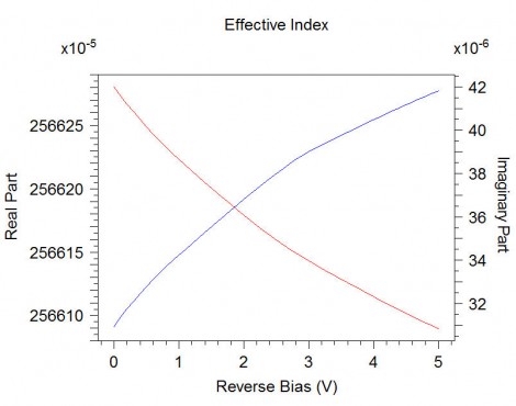
Figure 3: Electric effect of applied RF signal on optical mode
As observed, the change in effective index is very small, about 5x10⁻⁵/V at reverse bias and the VpL is about 1.5 V-cm. Therefore, the estimated length TW-MZM is about 8mm long with push-pull configuration and 1V bias. The discrepancy between the simulated results and those in reference 1 is expected since some of the details of their structure were not reported.
Transmitter chip using the TW-MZM device
The RSoft OptSim Circuit layout of the transmitter using a TW-MZM is shown in Figure 4. The layout consists of IMEC foundry process design kit (PDK) elements for the photonic components and transmission line elements for the RF electrodes. A back-to-back receiver is used to estimate the performance of the transmitter chip. As mentioned previously, the performance of the TW-MZM depends on the matching between the effective index of the optical waveguide and the electrical transmission line. In addition, the traveling wave nature of the modulator makes it sensitive to reflections due to impedance mismatch in the traveling wave electrode. This case study focuses on the performance impairments due to the impedance mismatches as a result of variations in the fabrication process. The impedance mismatch can be between the generator and the phase shifter electrode, or between the phase shifter electrode and the load, or both. A similar study can be carried out to estimate the impact due to foundry process induced variations in the effective indices of optical and RF modes.
The physical parameters of the device are taken from the device design discussed in the previous section, and Monte Carlo scans are performed over the impedances to estimate the performance impact.
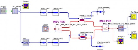
Figure 4: Layout of the transmitter chip using TW-MZM. Modulating data rate is 40Gbps. The back-to-back receiver is used for performance estimation.
Figure 5 shows the effect of the impedance between the electrode and the load on the modulator’s extinction ratio as measured from the optical eye at the modulator output.
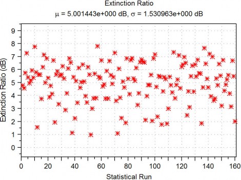
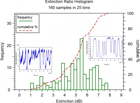
Figure 5: Distribution (top) and histogram (bottom) for the extinction ratio at the modulator output
The extinction ratio varies from as low as 1 dB to as high as 8 dB. Figure 6 shows the effect of the impedance mismatch between the electrode and the load on the bit error rate (BER) of the back-to-back received signal at the modulator.
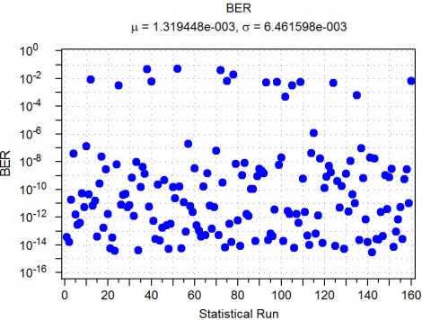
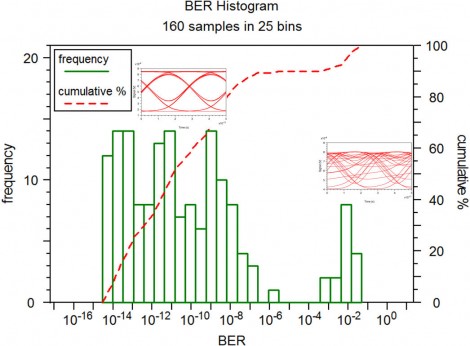
Figure 6: Distribution (top) and histogram (bottom) for the BER at back-to-back received signal
While the BER mostly lies in the 10-10 to 10-14 range, it goes as high as 0.1 and as low as 10-15 due to the stochastic nature of the process variations.
It is important to take into account the tolerances in the fabrication process, since it not only helps photonic foundries estimate the yield, but also helps system and chip designers understand performance bounds. Modeling at the device and circuit levels provides unique granularity in learning the most sensitive design parameters that are susceptible to prevalent foundry technologies and are likely to have the greatest impact on process yields and overall performance.
Reference: Baehr-Jones, Tom, et al. "Ultralow drive voltage silicon traveling-wave modulator." Optics Express 20.11 (2012): 12014-12020.
Written by Jigesh Patel, Enrico Ghillino, Chenglin Xu, Dan Herrmann, and Evan Heller, Synopsys Inc.












 Back to Features