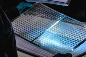
Silicon inspection can be a challenging problem for silicon and semi-conductor manufacturers in terms of pattern alignment, pattern defect inspection and edge position bonding inspection. During the manufacturing process, foreign particles and defects may appear on the top, bottom, inside or in between the wafers. And as the thickness of wafers get smaller, the backside defects are becoming more important to detect. They include trapped air, air pockets, micro-cracks and other fine features caused by photonic emissions. It is important to find the location of these defects. Defects do not initially affect the chips functionality, but they do end up affecting the chips reliability.
SWIR cameras
While front side defects can be detected using visual inspection how can backside defects be detected?
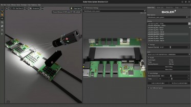
Silicon has an interesting property where it becomes translucent at wavelengths >1150nm. Because of this property, two dimensional FPA InGaAs cameras are ideal for detecting wafer defects. InGaAs cameras are capable of detecting light between 400nm and 1700nm in the Visible and Short Wavelength InfraRed (SWIR) range of the electromagnetic spectrum. With the use of filters, InGaAs cameras can limit the wavelength range they detect to only those where the wafers are translucent which makes them ideal to use for silicon wafer inspection, alignment and edge position bonding. (Figure 1)

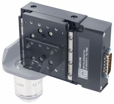
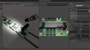
Raptor's OWL 640 II and OWL 1280 cameras are excellent candidates for this application. They combine a high sensitivity, large image area and high speed to allow for quicker inspections. And they are rugged and compact with stabilized cooling, ensuring reliability. These cameras have already been incorporated into several inspection system setups for customers in the semiconductor industry. (Figure 2)

The low noise and high sensitivity of Raptor Owl cameras allow for quick detection of any defects in the wafer, improving quality and reliability.

- Visible SWIR technology. Enables high sensitivity imaging from 0.4µm to 1.7µm
- High quality sensors. 99.5% operability, 640x512 15μm or 1280x1024 10μm •
- High Speed Imaging. Owl 640 II achieves 120 fps and the Owl 1280 achieve 60 fps
- On-board Automated Gain Control (AGC). Enables clear video in all light conditions
- On-board intelligent 3 point NUC. Enables highest quality images
- Active Image Enhancement. Further increases the image resolution of the 640x512 sensor
- Easy control of camera parameters. Control of Exposure, Gamma and intelligent AGC
- Ultra compact. Owl 640 II: 50x50x91mm/282g Owl 1280: 50x50x61mm/247g
- Rugged, fanless. Operation tested up to 2.3 teslas