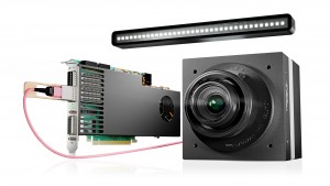


In electronics production laser system solutions not only help make the production of printed circuit boards, semiconductors, OLED displays or solar panels more efficient. Many steps would not be possible without laser light in this precision and fineness of the structures. "Through ever shorter wavelengths, constantly increasing performance and compliance with extreme reliability requirements, state-of-the-art laser systems continuously push the limits of what is possible in electronics and microelectronics production", confirms Gerhard Hein, President of the Laser and Laser Systems for Material Processing Working Group in the VDMA. The VDMA acts as the promotional supporter of LASYS which takes place in 2018 from 5 to 7 June in the exhibition halls of Messe Stuttgart.
Higher efficiency in solar cells
Diverse laser applications shape the electronics industry. For instance, the solar industry benefits greatly from material-removal laser structuring processes. Hein adds: "During the production of crystalline solar cells the laser removes passivation layers, separates the front and back electrically by edge isolation or inserts bore holes for contacting." The LASYS exhibitor 3D-Micromac manufactures machines for the photovoltaics area for the laser contact opening of high-efficiency PERC (Passivated Emitter Rear Cell) solar cells or for the thermal laser beam separation of solar wafers in half cells. "For both technologies the laser technology makes possible a higher degree of efficiency of the cell or the solar module. The use of half-cell technology enables the average module output of a solar module to increase by up to three percent and no crystal damage occurs at the separating edge", explains Mandy Gebhardt, Marketing/PR Team Leader at 3D-Micromac.
Vibration- and dust-free laser printed circuit board processing
The LASYS exhibitor InnoLas Photonics, for example, feels right at home in printed circuit board processing. It develops high-efficiency OEM lasers for laser cutting of contours and depanelling (separating) of fixed and flexible printed circuit boards, in addition to laser structuring of the copper top layer of printed circuit boards with a minimal effect on the material underneath. Martin Paster, Sales Manager at InnoLas Photonics, reports: "The beam sources developed especially by us for this laser process allow the highly efficient cutting of printed circuit boards. Laser solves the two main problems of the conventional processing methods of sawing and milling, namely vibrations and dust development. With the use of the contact-free and thus vibration-free laser cutting process the undesired dust development can be reduced by over 90%. A huge advantage for the manufacturer of electronics circuits and sensors."
Laser cutting and drilling with ultimate precision
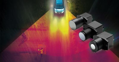
In the manufacture of smartphones and tablets laser performs the cutting and drilling of hardened glass for touch-sensitive screens. "With our high-tech scan heads (5 to 8 axles) precision bore holes can be made with customer-specific, totally reproducible drilling geometries and flank angles – challenging cutting applications can also be performed with precise control of the angle of the flanks", states Barbara Gößwein, Marketing Manager at Arges.
Separating OLED layer materials without causing damage
A current trend in the display industry is flexible displays based on OLED (Organic Light Emitting Diode) technology. Kian Janami, Industry Management Microprocessing at Trumpf, explains: "These displays should only be exposed to minimal mechanical stress in the manufacturing process in order to not damage the sensitive functional layers and thus not affect the performance of the displays." The LASYS exhibitor Trumpf manages this with ultrashort laser pulses in the femto and picosecond range. "The different layer materials can be separated at extremely high peak outputs", adds Janami, "without any mechanical effects. At the same time the process is extremely precise in order to respond to the increasingly smaller structures Different wavelengths in the infrared, green or UV spectrum ensure that the properties of laser can be optimally adapted to the materials.
Even finer structures in the future
Hein mentions another application, laser annealing, where laser is indispensable: "Here the charge carrier mobility is significantly increased, which marks a decisive step for the production of high-resolution LCD and OLED displays." According to Hein, the option to use flexible substrates continuously expands the application field for laser systems:
"So-called AMOLED displays (Active Matrix OLED) are a real challenge due to the very high resolutions and extremely broad colour spectrum in the range of mobile displays." Janami predicts: "In the future the structures in semiconductor, OLED or solar panel production will become finer and finer and the requirements of the beam sources will become correspondingly higher. The appropriate beam shape will play a big role here in the future because with it the productivity requirements of the user can be fulfilled." And laser also sets the tone in semiconductor lithography. "Key phrases here are DUV microlithography (Deep ultraviolet) for the manufacture of highly integrated circuits and EUV microlithography (Extreme ultraviolet) for the production of semiconductor chips with structure sizes below 10 nanometres", summarises Hein.
LASYS 2018: Concentrated know-how and expertise under the one roof
Concentrated laser expertise under the one roof, high visitor and location quality in the heart of important industrial sectors, increasing international character – find this and a whole lot more at the upcoming LASYS. Every two years exhibitors and those interested in laser material processing get together in the halls of Messe Stuttgart.
LASYS 2018 will be held at the Stuttgart trade fair centre from 5 to 7 June 2018.
For further information, visit: www.lasys-messe.de.