


Historically, CCD technology has an intrinsic advantage when it comes to TDI applications. CCDs operate by shifting charge from pixel to pixel across the image sensor. This allows the ability to add multiple samples (e.g. pixel lines in a multi-line camera) without complex circuitry to perform the integration operation and the noise penalty that would come with it. But the CCD technology is pricey to fabricate, output data rates are slow, and imaging devices that use it consume much more power than comparably-sized CMOS devices.
With CMOS processes, this type of charge transfer across multiple pixels has not been possible. Instead the signal charge is converted to a voltage directly in each pixel – the resulting voltage signal is amplified and read out from the chip periphery. Where CMOS shines is the way in which it deals with these signals – speed, power, noise, and ultimately cost are all superior to what can be achieved with CCD technology. These advantages are complemented by the feasibility of placing additional functions right on the sensor chip, by robust behavior under ionizing radiation, simpler system design, and convenient access to CMOS manufacturing capacities. Ultimately this makes for a simpler device that is cheaper to make and run. This explains the dominance of CMOS technology in almost every image sensing application except TDI.

The requirement that the signal be read out of the pixel as voltage is what makes the implementation of TDI functionality in CMOS image sensors difficult. That’s why, even though JPL announced CMOS image sensors capable of TDI fifteen years ago, actual products remain rare. However, customer demand is clearly there, so despite daunting engineering challenges, several solutions exist, and other exciting solutions are on the way including (surprise!) the introduction of charge-based summing into CMOS processes. Where the solutions differ is in how signal summation happens, so let’s start by comparing those.
Charge summing in the pixel array
Traditionally, charge domain summation has been the architecture of choice for Time Delay and Integration or TDI. Charge is transferred between pixels, from one row to the next, synchronously with the movement of the scene. A single read operation is performed once the charge packet reaches the bottom of the pixel array. With a long history of development and intrinsic advantages for very low NEE (Noise Equivalent Exposure) with full well, and excellent sensitivity, charge summing enables high scanning speeds in light-starved applications. The averaging of many pixels in the TDI column produces images with good contrast and improved uniformity of photo-response and dark signal non-uniformities.
Another point in favor of charge summing is the rate of degradation in the modulation transfer function (MTF) due to the summing integration. In a charge summing operation, motion-related MTF due to discrete charge can be very close to the theoretical maximum.
Another point in favor of charge summing is the rate of degradation in the modulation transfer function (MTF) due to the summing integration. In charge summing operation, motion-related MTF due to discrete charge can be very close to the theoretical maximum. However there are downsides – transferring charge between pixels requires gates which are only partly transmissive to light. This results in lower quantum efficiency (QE), particularly at short wavelengths. Backside illumination can improve performance here, but at the cost of more expensive silicon processing.
And of course the biggest downside is that the transfer of charge required to perform charge summing has not been available in CMOS processes.
Summing off of the pixel array
We have already learned that charge transfer has not been possible in CMOS processes, so charge summing in the pixel array is not an option. Instead, solutions for TDI in the CMOS world have focused on doing the summation outside the pixel array in a memory array that has a number of memory elements identical to the number of pixels. The memory can be implemented in either the analog domain or the digital domain, and either on- or off-chip.
What is common to all of these is that the signal level is read out directly from each pixel as a voltage signal. Because summation takes place external to the pixel array, each and every pixel in the array must be read out each and every line time. For example, if the TDI line rate is 100 kHz, then the entire pixel array must be read out, pixel by pixel, every 10 ms. With a given number of pixel rows, the same number of read operations has to be performed to obtain a summed row. This increases the read noise by the square root of the number of pixel rows, and it increases the time required to process each row. There can be significant penalties compared to a charge based system, where the result is acquired with only one read operation.
Note that because these solutions require a memory array that has as many elements as the pixel array, additional real estate and power are required.
As mentioned, the memory can be implemented in the analog space or the digital space. In a typical analog approach, the pixel output levels are stored in column based capacitors as analog voltage levels and time-delay summed with active circuitry. In a fully digital system, the time-delay summation is performed in the digital domain. This makes the memory elements more immune to external disturbances, and routing can be simpler, however it requires that each read operation be accompanied by a digitization operation which further impacts noise and speed. In contrast to a fully digital solution, the analog approach requires only one digital conversion per line.
One advantage of a fully digital architecture is the fact that the in-pixel conversion gain can be maximized, without compromising the dynamic range under bright conditions. While an analog voltage summation scheme is limited by the signal swing and a charge-based solution by the charge handling capacity, a digital architecture is only limited by the available bit space after the addition. Also, it is easier to add pixel rows with the digital solution (if the ADC is fast enough) compared to the voltage-based solution. Adding pixel rows is attractive, since the total collected photons scale much faster than accumulated read noise. However, more rows require a fast ADC and complex processing/addition logic to perform the TDI summing. For a column having N rows, the ADC must process all N rows at the TDI line rate, which limits the number of rows in the pixel array performing TDI. Using faster ADCs is a trade-off between introducing more complexity (and circuit area and power) and more noise, which is not ideal for TDI applications.
Despite these challenges, performing TDI summation outside the pixel array, either with an analog or a digital memory, can provide some significant advantages. In addition to the signal capacity advantage just described, external summing allows conventional CMOS pixels to be used in the pixel array, and that allows for functionalities like Electronic Exposure Control (EEC) that are not typically possible with charge summing solutions. This is an important advantage in many emerging machine vision applications where multiple light sources are used to gather different types of information from the scene during a single scan.
Charge summing revisited
Charge-based summing of multiple pixel rows has typically been based in CCD technology. It is the only technology where it’s been possible to physically move charge between adjacent pixels. However, this is changing, as some of the process blocks common in CCD; like buried channel pixel structures, are being migrated to CMOS processes. This makes charge summing possible on a CMOS substrate, albeit with the constraint of lower clock voltages which necessarily restrict charge handling capacity. These constraints show up to users as limitations in maximum signal size, and therefore as limitations in dynamic range. However the much lower read noise levels achievable with CMOS readouts versus CCD readouts (significantly lower achievable NEE), as well as lower power dissipation and higher data output rates, make this a very compelling technology choice for many applications. And while this technology is still in its infancy, it offers promise for future product development.
Hybrid architectures
Where the limitations in charge capacity (maximum signal size) inherent with CMOS charge summing solutions are too restrictive, hybrid approaches where charge summing is combined with voltage or digital summing may prove interesting. As CMOS processes start to offer multi-pixel charge transfer capability, these hybrid architectures will also become attractive solutions.

Such hybrid architectures reveal totally new opportunities and compromises to balance in a camera solution. For example, in a charge-based architecture, the handling capacity of the pixel and the transfer operations define the dynamic range under bright conditions. Also, adding pixel rows improves the sensitivity and with it the NEE, but it does not increase the full well. If a digital summing stage is introduced to add the results of two charge summing pixel arrays, the total number of collected photons is doubled. Although adding a read operation and AD conversation for digital summing will compromise NEE by a factor of root-2, the maximum signal is doubled, resulting in a net larger dynamic range under bright conditions. Adding digital summation to the charge based TDI architecture offers a way to extend the full well faster than the degradation in noise, resulting in a net lower dynamic range. Depending on the application and the system you’re developing, some of this might be music to your ears.
All engineering is intelligent compromise
As CCD becomes a smaller and smaller part of the market, and as CMOS technologies allow for summing within the pixel array and external to the pixel array, all of the above solutions will play a role. Most companies are focusing on one solution only, but the intrinsic limitations of the technology are telling us that this is a mistake. Each technology has its unique challenges and as an industry, we have a long path of development ahead of us. We will have both technologies, and considering the limitations of charge domain CMOS TDI, there will still be a requirement for both in the future.
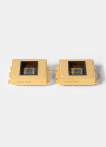
Piranha XL
E2v made an early TDI sensor in 2010 with charge transfer in a 0.18 um CMOS process. Another early attempt at CMOS TDI came from CMOSIS in 2011 for the CNES (the French National Space Agency) with a fifty-stage TDI solution. In that solution, speed and voltage stability became challenges. Though neither of these has appeared as a readily accessible product for machine vision customers, Dr. Lou Hermans at CMOSIS stated that “under certain conditions, CMOS TDI implementations will even outperform CCDs in terms of dynamic range and readout noise.”
Each technology has its unique challenges and as an industry, we have a long path of development ahead of us.
The Piranha XL is another step forward, offering high-performance TDI, built on a digital summation architecture. With very high resolution and 12 lines, intrinsic noise levels are overcome with very powerful on-chip processing. The result of a significant (and award-winning) engineering effort, much of the development required finding the right trade-offs between speed, artifacts and noise. And with the digital summing, each of the 12 lines contributes to the very high SNR in the light.
It may not sound like a motivational speech, but engineers know the truth: Compromise is the key to success. The technologies will continue to develop, and new balances will be found, expanding the opportunities for CMOS TDI in many industries.
Written by Eric Fox, Technical Director, CMOS Integrated Circuits, Teledyne Dalsa