Megatrend applications like 5G wireless technologies, electric vehicles, and advanced mobile devices demand miniaturization and extra functionality. Therefore, fabricating the next More than Moore (MtM) device generation requires tools with new technical specifications. These are very different to the “More Moore” mainstream semiconductor industry with respect to resolution, overlay, depth of focus (DOF), wafer bow and backside alignment.
MEMS, sensors and power devices have more relaxed specifications, so that mask aligner tools are sufficient at lower cost. However, megatrend applications are pushing devices with more stringent requirements, with lithographic features below 1μm. This would pave the way towards greater adoption of stepper tools.
Wafer-to-Wafer (W2W) bonding is fueled by MtM devices. It’s currently supported by CMOS Image Sensors (CIS) based on fusion bonding, which enables Phase Difference Auto Focus (PDAF) as well as faster shooting. Nevertheless, W2W process growth will be led mainly by potentially integrating hybrid bonding with no Through-Silicon Vias (TSVs).
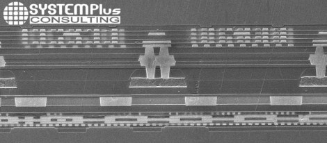
Hybrid Bonding - CIS Cross-Section - Rear Camera Module Samsung Galaxy S7. Source: Wafer to Wafer Permanent Bonding Comparison 2018 report, System Plus Consulting
Such processes could be used in new consumer CIS approaches such as global shutter and Time-of-Flight (ToF) technology and also the automotive industry in advanced driver-assistance systems (ADAS). Looking ahead, emerging mainstream products such as 3D NAND memory and 3D Systems on Chips (SoCs) are expected to reshuffle the W2W business in the next few years. They will replace die-to-wafer (D2W) and wire bonding, in order to maximize the number of memory cells and yield and solve stacking layer limitations.
We had expected W2W production to pick up earlier for 3D DRAM stacked memories. However, in reality, cost and technical aspects today firmly limit adoption of W2W to replace D2W assembly methods.
The “Bonding and Lithography Equipment Market for More than Moore Devices” report presents a comprehensive overview of the status of the three equipment types used for MtM devices, along with a more in-depth analysis of technology trends and impacts made by the megatrend applications.
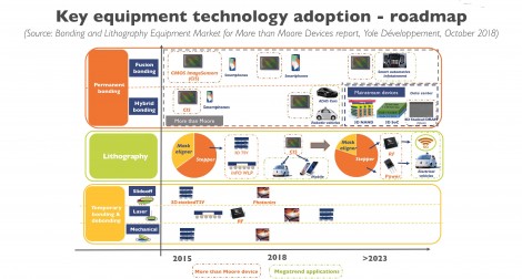
More than Moore industry manufacturing complexity brings new business opportunities in bonding and lithography equipment markets
The overall semiconductor equipment market is worth several billion dollars. By contrast, the permanent bonding, temporary bonding and debonding and lithography equipment market for the MtM industry is a small niche representing millions of dollars.
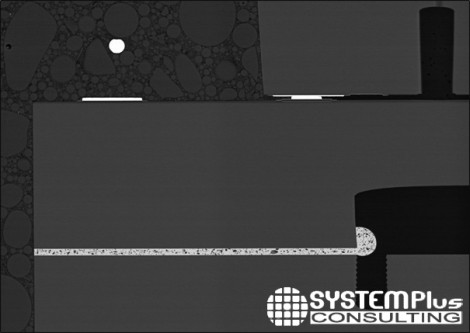
Glass Frit & Thermo-compression Bonding - Pressure Sensor Cross-Section - STMicroelectronics LPS22HB. Source: Wafer to Wafer Permanent Bonding Comparison 2018 report, System Plus Consulting
However, megatrend markets push MtM devices to new levels of complexity, resulting in big investments. Consequently, the total equipment market for these process steps generated revenue of more than $400M in 2017. It is expected to peak at ~$750M by 2023, with a 10% compound annual growth rate (CAGR) over this period. This is mostly driven by lithography, followed by W2W permanent bonding.
The new lithography equipment market for MtM devices is mostly driven by advanced packaging. This sector accounts today for almost 60% of the overall MtM lithography tools market and will continue dominating this industry with stepper technology.
Meanwhile, a high percentage of lithography equipment revenue for MEMS and sensors, CIS and power devices comes is generated by retrofitted tools coming from the legacy semiconductor industry. Nevertheless, new lithography systems will be shipped to meet smaller alignment and feature sizes, where older tools will face limitations.
The W2W bonding market is mostly driven by CIS imaging and is expected to be fueled by emerging CIS products. However, new mainstream semiconductor applications such as 3D NAND and 3D SoC will also strongly push W2W bonding market growth over the next five years.
Temporary bonding and debonding still represents a rather small niche reaching more than $55M revenue in 2017. Yet it‘s been already applied in numerous MtM areas such as 3D TSV platforms, fan-out wafer level packaging (FO WLP), MEMS and sensors, power devices and photonics applications.
From a technology point of view, laser debonding represents the dominant technology widely used today for FO WLP and 2.5D interposer packaging. It is expected to remain the leading process, mainly supported by the major memory manufacturers such as Samsung, SK Hynix and Micron. These companies are expecting to transition from mechanical debonding/slideoff debonding to laser debonding for the next generation of HBM2 memory due to yield issues and to support the future high volume production forecasted by end of 2019.
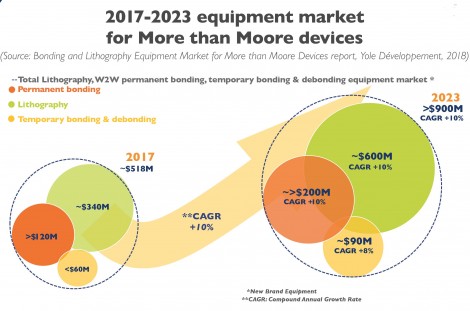
More than Moore devices lead to a much broader bonding and lithography landscape
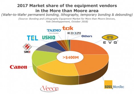
When looking at the competitive landscape, the MtM equipment market is diversified, with groups of equipment vendors coming from different angles.
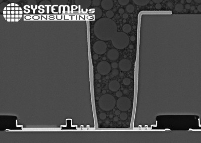
Thermo-compression - RF Filter - Broadcom AFEM-8072. Source: Wafer to Wafer Permanent Bonding Comparison 2018 report, System Plus Consulting
As such, the bonding equipment market is highly concentrated under the control of specialist equipment suppliers, like EVG and SUSS MicroTec. These companies have developed expertise in very specific equipment lines where legacy equipment suppliers do not have the capabilities to support such processes. The exception is Tokyo Electron Limited (TEL), which is very active in the permanent bonding equipment.
In contrast, the lithography equipment landscape for MtM devices is fragmented in different ways since it is served by two main company types:
- Specialist equipment vendors like Veeco, EVG, SUSS Microtec, SMEE, who offer brand new lithography tools specifically for the MtM industry
- Top-tier semiconductor equipment suppliers like ASML, Canon, Nikon, mostly supporting refurbished equipment
However, the equipment landscape is currently evolving towards greater diversification in both bonding and lithography. For instance, Asian equipment vendors have recently created strong price pressure and could reshuffle the MtM equipment market. New Chinese local players benefit from strong subsidies from local governments. They have entered the market and started competing with the top players. SMEE today is the dominant Chinese company, holding around 70% market share of the domestic LED market in terms of volume, providing low-cost bonding and lithography.
Some other Asian equipment suppliers include Korean company EO Technics, and Taiwanese company Kinyoup Optronics, offering laser debonding processes mostly dedicated to FO WLP.
Meanwhile, in the quest to acquire market share in the MtM industry, large semiconductor Front-End or Back-End equipment suppliers have adopted different strategies. They are expanding their lithography activities through acquisitions of other companies to diversify and complete their product portfolio. For example, ASML spin-off Liteq was acquired by Kulicke & Soffa, Veeco bought Ultratech and KLA Tencor purchased Orbotech.
Finally, Canon, a key front-end lithography equipment supplier, is challenging MtM suppliers by developing brand new tools at a reasonable cost. In addition, they recently skipped a step in the bonding business by leveraging their physical vapor deposition (PVD) capabilities to launch a permanent bonding tool based on metal interfaces.
Written by Amandine Pizzagalli, Technology & Market Analyst, Yole Développement - Audrey Lahrach, Cost Analyst, System Plus Consulting















 Back to Features