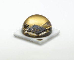
Photonic integrated circuit technology, deployed in the transceiver market for datacenters, will likely become a solution for next-generation, low-cost and compact lidars for applications including autonomous cars. The lidar market was steady for a while in the past few years when the innovation level was not keeping up with the market needs (e.g., lowering the cost, more compact and high-performance devices). The biggest trends we are seeing now, is the drive to meet these demands via volume wafer-scale manufacturing in CMOS pilot lines.
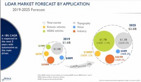
Figure 1: Lidar market forecast by Yole, 2020.
Cost reduction
Cost reduction is happening both on the manufacturing side by integrating more components on the same chip (e.g., photodiodes, and light sources) and on the maintenance side by eliminating mechanical parts (solid state lidars). This is the same trend we have seen for the electronic industry, meaning moving from discrete components (transistors, resistor, capacitors) toward integrated ICs with millions of components. Here we are focusing on integrated photonic circuit (PIC) based lidar, which is a compact form of solid state lidars. Today photonic integrated circuit technology is deployed heavily in the transceiver market for datacentres (backbone of our daily internet) and we strongly believe it will be a preferred solution for next gen low cost and compact lidars for many applications including autonomous cars.
At imec, we are working on the general topic of “Optical BeamForming (OBF)” using integrated photonics where specific application domain becomes lidar, communication, earth observation, etc (Figure 2). As shown in this figure, the main driver for the OBF is the automotive lidar market , which has attracted many players including giant semiconductor players like Intel, Samsung, as well as many successful start-ups such as Scantinel.
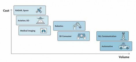
Figure 2: The main driver for the OBF is the automotive lidar market , which has attracted many players including giant semiconductor players.
In this context, lets review what imec engineers have achieved so far.
First of all, at imec we have demonstrated 2D lidar scanners with on-chip readout and adjustable angular access. First generation of the OPA was only 32 channels where recently we have demonstrated more than 500 channels on the single chip. This shows the scalability of the wafer scale approach at one hand and on the other hand express imec flexibility to collaborate with our customers to meet their specific requirements. In the same photonics platforms, we have also succeeded in the generation of complex structured light for multi-spot scanning approach, which is similar to lidar concept on the demonstrated lidars on smartphones.

Figure 3: Comparison between Standard Flash lidar and Structured light system performance (top). (source), scanning single beam via 32 channel imec OPA (bottom left), scannable structured light illumination (bottom right).
Si-based photodiodes
Second, the imec photonic team have also demonstrated integrated Si-based photodiodes as an on-chip phase readout for on-chip calibration. This is an important step toward simplifying full system calibration and also recalibration.
Figure 4: Cross section of Si PN junction photodiode used for on-chip calibration at C-band (top), 32 channel OPA transmitter based on Si photonic on-chip phase interrogator and on-chip SI photodiode for calibration purpose (bottom).
Two mature platforms
Finally, on the technology side, two mature 200 mm platforms have been set up: First photonic technology platform is our SiN photonic line, which is low loss and has high power handling capability. Quality of the processing is so incredibly high, which we can reach less than 1 nm topography on the SiN film on the 8 inch wafer. Second is hybrid cointegration SiN/Si platform with all advantages of the SiN layer plus state of the art high speed devices and dense integration capability.
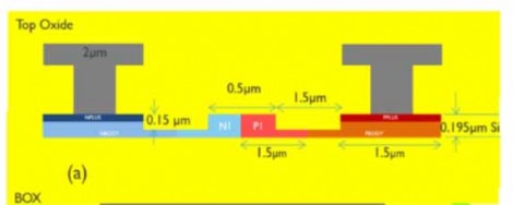
Figure 5: Si photonic technology with co-integrated SiN layer (top-left), leaky wave antenna concept using SiN/Si integration (top-right), high quality SiN technology with extreme low loss capability (bottom-left) and basic building blocks available in this platform (bottom right).
The current focus at imec is on the photonic integrated circuit technology development to offer the best available technology to realize customer needs. To make a lidar so compact based on the integrated chip, our customers are asking for the integrated laser source, low loss, low power phase shifter, switching network, waveguide and finally integrated PD. The similar type of integrated technology can be used not only for a next-generation lidar scanner for autonomous cars, but also advance dynamic imaging, spectroscopy systems and for flexible bandwidth 5G and communication applications.
Written by Marcus Dahlem, Principal member of technical staff, imec.












 Back to Features