


The European photonics market is estimated to be worth €90 billion, according to a recent survey by Tematys, which highlights the impact that photonics has on mega-markets and application areas. The survey, Exploration of Photonics Markets was published by Photonics21, and it looked at projects funded in part by the EU and private enterprises. Some of the important application areas served by European photonics companies include the environment, additive manufacturing, medicine and health, manufacturing, lidar and autonomous technologies.
Many of these hot application areas are driven by societal changes, noted Benno Oderkerk, CEO of Avantes, a specialist in fiber-optical spectroscopy instruments and systems. Some of these changes include environmental challenges and an aging society, which give rise to trends in mobility, food safety and more. Avantes, in collaboration with many other photonics peer companies, is playing an active role in supporting these new applications with spectroscopy instrumentation and know how.
The environment and sustainability
Protecting the climate by reducing global warming is one of the greatest challenges of our time. The Paris Agreement set the target for a temperature rise of significantly below 2 degrees Celsius, compared to pre-industrial levels. Photonics applications are helping to meet this target as they are expected to contribute 3 billion tons less Co2 per year by 2030, according to a recent study, Light as the key to global environment sustainability, by Spectaris, the Fraunhofer Institute, Tematys and Messe Munchen. Dr. Bernhard Ohnesorge, Managing Director Carl Zeiss Jena GmbH and Chairman of the Photonics Trade Association Spectaris e.V. said, “Photonics has made it possible to identify the hazards of climate change. It gives us the tools to protect our world. What matters now is that we make sure to use these opportunities wisely.”

The study provides eight examples of photonic applications that contribute to environmental sustainability:
- Photovoltaics
- LED lighting
- Optical communication in data centers
- Fiber optic communication networks
- Energy-efficient displays
- Optical early detection of forest fires
- Laser-supported metal recycling
- Optical communication in 5G mobile networks
A ninth application is the acquisition of climate data, and one example is a European photonics initiative by a group from the Leibniz-Institute of Atmospheric Physics and the Fraunhofer Institute for Laser Technology ILT, both in Germany. The scientists are developing a lidar network that will be able to deliver climate data continuously and on a large scale. The system is the size of a washing machine and, thanks to its innovative laser design, is virtually maintenance-free. In addition to a smaller size, its energy consumption has also been reduced by a factor of 100 and is now under 500 watts. Parts of the laser were manufactured cost effectively with a 3D printer. With the new, stable laser technology, many measurements will be possible, for example, with the system on airplanes it can measure the distribution of volcanic dust in the atmosphere or satellite-based to collect global climate data.
Photonics-based solutions can contribute to sustainability through reduced energy consumption, lowering carbon emissions, reducing use of toxic materials, by enabling new recycling processing, by contributing to renewable energy generation and other technologies that will protect the environment.
Additive manufacturing
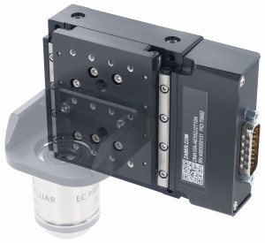
Additive manufacturing or 3D printing is forecast to be growing at more than 26% a year through 2023. It´s being used in everything from metal parts manufacturing in the automotive industry, to design and manufacturing of custom optics, to the fabrication of artificial limbs, blood vessels and heart valves. Lasers play a significant role in this application area because they focus large amounts of energy on a wide range of material powders, fusing them into 3D parts. Laser Powder Bed Fusion (LPBF), also known as Selective Laser Melting (SLM), is a process in focus in the AutoAdd project the Fraunhofer Institute for Laser Technology ILT. The project intends to make it easier for the automotive industry to use additive manufacturing by integrating the LPF process chain in the automotive mass production environment reduce unit costs.

Scanlab GmbH is a German manufacturer of galvanometer scanners, which are finding a home in additive manufacturing, according to Stefan Recht, Teamleader, Technical Sales Europe. Recht said, “One trend we see is that machine integrators work more intensively on developing multi-head laser machines, e.g., for additive manufacturing. This is because productivity for large-area workpieces in particular can be significantly enhanced by combining multiple scan systems with high-overlap image fields.“ Scanlab’s fiberSYS system is a turn-key solution that is designed to simplify machine construction.
One challenge of additive manufacturing is the ability to print at the micrometer scale at high speed. A research project at Karlsruhe Institute of Technology (KIT) in Germany is working on a system that may overcome this challenge by printing highly precise, centimeter-sized objects with sub-micrometer details at a so far unmatched speed.
Read more about this work in “Fastest High-Precision 3D Printer”.
Medicine, health and life sciences
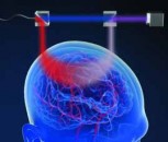
One of the societal changes is our aging population, which has increased healthcare needs—giving rise to advanced imaging, non-invasive surgeries, and other light-based medical applications. The use of light-based technologies is enhancing lives by aiding in early detection and treatment. For example, cancer is among the leading causes of death worldwide, death rates for individual cancer types have declined in part due to advanced research on light technologies such as fluorescent imaging that helps in cancer detection and photodynamic therapy used in treatment.
To this end, there is an effort underway In Europe to accelerate development of light-based diagnostic devices. The European Commission is expanding the existing photonics pilot line offering by funding the establishment of MedPhab pilot-line under Horizon 2020, the Framework Programme for Research and Innovation.
Optical microscopes are indispensable photonics tools in the areas of life sciences and diagnostics. According to Dr. Ute Hofmann, Product Manager Bioimaging at Jenoptik Optical Systems GmbH in Germany, “From cellular imaging to molecular biology, from interactions of proteins, genes and biomolecules in basic research to pharmacological responses in high-content screening, from tissue and biopsy imaging to surgical imaging – microscopy and digital imaging is central to life sciences research, as well as clinical diagnosis and drug discovery. Making the unknown visible is the overall challenge in these disciplines and the key for success."

While traditional microscopes or integrated into benchtop devices can pose a challenge due to size, cost or usability, Jenoptik’s digital microscope subsystem Jenoptik Syions is an example of a new trend in microscopy and digital imaging. It was designed to be versatile, take up minimal space, be easy to integrate and economical. Made for flexible integration into new or existing instruments and thereby eliminating interface issues, Jenoptik Syions enables benchtop devices to use or expand with superior digital imaging capability. Customers can choose from a set of highly configurable modules for light sources, optics and electronics, sensors and software tailored to the application needs, e.g., bright field or fluorescence imaging.
Berliner Glas is expecting further miniaturization in tools as well as medical and technological progress of imaging modalities, such as fluorescence imaging as well as multispectral and hyperspectral imaging.
Also, as the result of the increasing digitalization software, apps and robotic technology will see increasing use in the future. With a continued investment into micro-alignment, micro-optics and with its strategic partners in sensors and electronics, "Berliner Glas sees itself well-positioned to serve the requirements of its customers in the future", according to Wencke Schulz, Marking and Communications at Berliner Glas.
In addition, "we see an increase in regulatory requirements (medical device regulation) from 2020 on. Berliner Glas has been certified according to ISO 13485 for many years and our QM/RA department follows the new developments very closely," Schulz noted.
Manufacturing and materials processing
Today’s world of connected manufacturing is called Industry 4.0 or the Industrial Internet of Things (IIOT). To run a “smart factory” in which automation and connectivity are the backbone, many procedures and technologies must be reviewed and/or adopted. These may include robotics, augmented reality, embedded vision, cameras, sensors and even smart glasses, all of which present tremendous opportunity for photonics providers. 5G, the next generation of mobile telecom technology, will also play a role. Read “Technologies and Processes for Industry 4.0,” for more detail.
Ericsson has been working on a Swedish government-supported projects with SKF, a bearing manufacturer, and Chalmers University of Technology, to develop a network that can allow for custom products. They’ve found that 5G offers superior connectivity from the production floor to video conferencing in the meeting rooms.
Jenoptik offers products and solutions ranging from laser beam sources to optical systems, including all steps on the value chain for today’s manufacturing and materials processing applications. For example, with one of Jenoptik’s new plug and play systems, JENvelt, which combines a 2D galvo scanner, F-Theta lens and camera with an intelligent image processing software. These systems enable manufacturers to quickly and easily integrate laser processing machines, while fulfilling customer needs for Industry 4.0 capabilities, which include intelligent image processing and support for data handling, monitoring and process control.
SICK, a German- based sensor manufacturer, offers smart logistics solutions with cloud-based connectivity for safety sensors in human-robot collaboration and accurate track and trace systems on conveyers. These intralogistics applications are helping to bring logistics processes into Industry 4.0.
Opportunities in this market are far-reaching, as manufacturers recognize the increased throughput, customization capability and quality assurance

improvements in Industry 4.0. For this reason, a future focus for Jenoptik is on more integrated plug-and-produce optical systems. To get systems “ready for plug-in” is an advantage in the fast-growing markets and requirements to more flexible production, said Steffen Reinl, Senior Sales & Product Manager, Jenoptik Optical Systems GmbH.
Another focus, Reinl said, is on flexible optic solutions, e.g., changeable or customizable laser beam shaping. The future laser material processing equipment needs to be variable, because of different product materials, shapes and sizes – at best processed on one machine. And for Jenoptik, the third focus is on smartness and intelligent software-supported (imaging) systems. Laser manufacturers are challenged by product tolerances, such as those in shapes, and must fulfill the requirements for stable reproducible and repeatable quality.
The future looks bright for photonics companies serving this market. Jean Caron, VP of Sales and Support at Euresys, in Belgium, sees continued, strong demand. “The interconnectivity of the machines and production plants with the development of industry 4.0 will increase the demand for more intelligent and autonomous machine vision systems to help in increasing the smart automation of factories,” said Caron.
Lidar for autonomous driving
The automotive lidar market is poised to surpass $2.3 billion in the next seven years, or a growth rate of 35%, according to a recent report. Lidar is used as a part of ADAS sensors, giving cars autonomous capability, and we’re seeing many entrants in this rapidly growing field.

The expansion is the result of innovative product launches, trends in miniaturization and growing vehicle safety awareness across the globe. The European New Car Assessment Program is helping to drive the global autonomous market, as lidar is becoming a mandatory safety measure in automobiles.
Laser Components is a European photonics company with a range of lidar solutions. On the emitter side, its pulsed laser diodes provide the high-power, short-pulsed laser bursts that are the foundation in time-of-flight based range finding. On the detector side, Laser Components offers various configurations to detect the back-reflected signals.
The opportunities are great and competition stiff right now in the autonomous realm. “For the customer, autonomous technologies present a wealth of opportunities for camera and sensor manufacturers,” noted Ferdinand Reitze, Product Manager 3D at Framos in Germany. For example, with its Intel RealSense relationship, Framos showed easy to integrate 3D depth cameras and modules that are optional for autonomous devices such as robots, drones, other “seeing” machines and devices. Newly developed 3D depth cameras work, among other software applications, with the cubemos (a Framos spin-off) AI Skeleton Tracking SDK - a technology for 2D and 3D detection of people and their posture.
Several technologies are competing against each other for the same applications, including active stereo vs TOF vs structured light vs lidar 3D cameras. Guillaume Delpont, Product Manager at PicoQuant, a German laser manufacturer, said while there are different approaches being developed, tested and optimized…”at some point, probably one of a few of these approaches will be established and go into industrial production.”
“For customers it can be difficult to choose the technology that is best suited to meet their requirements for a specific application., “ said Framos’ Reitze. For manufacturers, however, the plethora of choices offers an opportunity to differentiate themselves and the company’s solutions. A challenge to entering this market, according to Peggy Dietrich, Product Manager Lidar Components, Jenoptik Optical Systems GmbH, is the lack of testing standards and scenarios that are the basis for the functional requirements of real-world lidar systems, e.g., detection range and image resolution. “While the market entrance risks for tier 1 system providers are high, Jenoptik decided to act as component or customized sub-system provider on tier 3 or tier 2 level,” Dietrich said. She noted that the potential is for very high-volume component sales. “If the lidar market reaches only a fraction of what some market analysts predict, the demand for “smart” moving objects (cars, drones, robots...) will go through the roof, as will the demand for their guidance systems which rely on our components.”
What the future holds
We’ve highlighted five of the most significant application areas being served today by European photonics manufacturers. Certainly, there are many more, with quantum technologies and semiconductors also on that list. The advancements in quantum communication are necessary for security, and there are a number of initiatives, such as the EU’s Quantum Technology Flagship initiative that developed prototypes using quantum encryption protocols to create secure transmission of sensitive information through the internet.

As for the semiconductor market, Dr. Johann Weinhaendler, Managing Director of ASM Amicra Microtechnologies, based in Germany, said in a recent interview with EPIC’s Jose Pozo that most of the larger semiconductor companies are combining photonics technologies. Carlos Lee, EPIC CEO echoed that sentiment: “Photonics is finally becoming a semicon technology. In particular 3 trends have been growing increasingly for EPIC Members: wafer-level co-packaging of optics and photonics (VCSELs, Silicon Photonics, MicroOptics, etc.), new solutions for fast 3D printing matching Industry 4.1 needs, and miniaturization and cost reduction of high power laser systems for consumer product manufacturing. We expect that the thin line between semiconductor manufacturing and photonics to become ever so thin and disappear.”
For European photonics companies to compete in these leading application areas, they must innovate and always be ready to meet customer needs, especially when customization is necessary. Being geographically close to the customer is an advantage, said Andreas Kunz, Business Director, Advanced Optical Components at Swiss-based Fisba. “For some products it is challenging to compete with low wage countries. It is still an advantage to be close to the customer with all the experts from R+D and production, as Fisba mainly does customized products for which we jointly develop the best technical and economical solution with the customer.” He noted that proximity is especially important when serving the defense market. “It is a great advantage being a European company with R+D and production in Europe when serving European Defense companies.”
While being located close to customers works well for building relationships as well as customized products, the photonics supply chain is increasingly global and affected by international issues. Last year the issue was the US/China tariffs, which sent a ripple effect through all photonic supply chains. This year it is COVID-19, which has shuttered factories and sent workers home, slowing production of a range of products that serve photonics manufacturers. Looking at where the components manufacturers are located, 52% are in Asia, 24% in Europe, 23% in North America and 1% in ROW. With COVID-19 affecting manufacturing in China, the result could delay manufacturing and shipment of critical components for manufacturers throughout the value chain. However, it will not undermine the very real need for photonic components globally. SPIE recently estimated that revenues for 2020 will reach $328 billion, which is an increase of 16% over 2018. The broad diversity of products serving application areas that are integral for daily life, the opportunities for European photonics manufacturers are strong and growing.
Written by Anne Fischer, Managing Editor, Novus Light Technologies Today