


Understanding the source and orientation of light in light-emitting thin films could lead to better light-emitting diodes (LEDs), solar cells and other devices that use layered nanomaterials. A multi-university research team has used a new spectroscopic method, called “energy-momentum” spectroscopy, to gain a key insight into how light is emitted from layered nanomaterials and other thin films.
The research, published online in the article “Orientation of luminescent excitons in layered nanomaterials“ in Nature Nanotechnology, was a collaborative effort of Brown University in Providence, Rhode Island (US); Case Western Reserve University in Cleveland, Ohio (US); Columbia University in New York, New York (US); and University of California-Santa Barbara (UCSB) in Santa Barbara, California (US). This article was sourced from ScienceDaily‘s article, “New Spectroscopy Method Could Lead to Better Optical Devices Such as LEDs and Solar Cells,” which in turn came from materials provided by Brown University.
The technique enables researchers to look at the light emerging from a thin film and determine whether it is coming from emitters that are oriented along the plane of the film or from those oriented perpendicular to the film. Knowing the orientation of emitters could help engineers make better use of thin-film materials in optical devices, such as LEDs or solar cells.
This new technique takes advantage of a fundamental property of thin films: interference. Interference effects can be seen in the rainbow colours visible on the surface of soap bubbles or oil slicks. Scientists can analyse how light constructively and destructively interferes at different angles to draw conclusions about the film itself: How thick is it? for example. This technique takes that kind of analysis one step further for light-emitting thin films.
“The key difference in our technique is we’re looking at the energy, as well as the angle and polarisation at which light is emitted,” said Rashid Zia, assistant professor of engineering at Brown University and one of the study’s lead authors. “We can relate these different angles to distinct orientations of emitters in the film. At some angles and polarisations, we see only the light emission from in-plane emitters, while at other angles and polarisations we see only light originating from out-of-plane emitters.”
The researchers demonstrated their technique on two important thin-film materials: molybdenum-disulfide (MoS2) and 3,4,9,10-perylentetracarbonsäuredianhydrid (PTCDA). Each of these represents a class of materials that shows promise for optical applications: MoS2 is a two-dimensional (2D) material similar to graphene and PTCDA is an organic semiconductor. The research showed that light emission from MoS2 occurs only from in-plane emitters. In PTCDA, light comes from two distinct species of emitters: one in-plane and one out-of-plane.
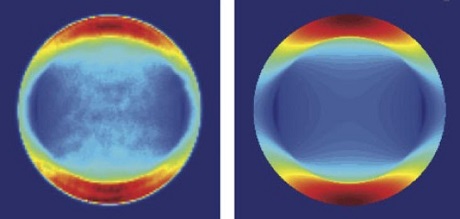
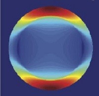
The orientation of light emission. The angular distribution of light emission from monolayer MoS2, left, closely matches the theoretical calculations for in-plane oriented emitters, right, indicating that light emission from MoS2 originates from in-plane oriented emitters. (Credit: Zia lab/Brown University)
Once the orientation of the emitters is known, Zia says, it may be possible to design structured devices that maximise those directional properties. In most applications, thin-film materials are layered on top of each other. The orientation of the emitters in each layer indicates whether electronic excitations are happening within each layer or across layers and that has implications for how such a device should be configured.
The same concept could apply to light-absorbing devices, such as solar cells. By understanding how the electronic excitations occur in the material, it could be possible to structure it in a way that converts more incoming light to electricity.
Funding for this work was provided by the US Air Force Office of Scientific Research, the US Department of Energy, the US National Science Foundation, and the Nanoelectronic Research Initiative of the Semiconductor Research Corporation.