


Photomasks – or photolithographic masks –are high-purity quartz or glass plates with precision images of integrated circuits designs. They have become inevitable as masters to transfer these images onto silicon wafers through optical lithography. This makes photomasks a key component in semiconductor chip manufacturing.
Integrated circuits are manufactured layer by layer; consequently the deposition or removal steps are repeated until the final circuit is completed. Each layer requires a unique photomask. The current generation of semiconductor chips commonly has 25-60 layers. State-of-the art lithographic equipment such as Deep-UV (DUV) Step-and-Scan systems project the light through the photomask and through an optical lens with a high numerical aperture. The intensity distribution of the light produces an image of the design on the wafer, which is coated with photoresist, a photosensitive material. By use of negative or positive photoresist material the unexposed/exposed areas of the material are removed in a post exposure development step so that thereafter the wafer can be etched or other materials can be applied.
Photomasks have become masters to transfer precision images of IC design onto silicon wafers through optical lithography.
Mask qualification and repair
Photomasks are complex products that are exposed to high energy densities during exposure. Still, as the integration density of semiconductor structures with the ever-decreasing feature sizes increases, also the precision requirements for photomasks steadily rise. Requirements of the semiconductor industry lead to a steady reduction in the lithography wavelength over the years from 248 nm to now commonly 193 nm to be able to create a structure of lower than 30 nm on the wafer.
Most lithographic photomasks in the semiconductor industry have a thin chromium oxide layer to provide better anti-reflective qualities. Finding and repairing of possible defects on the photomask is a major task, because these defects would be transmitted onto the wafer and create rejects. Companies such as Carl Zeiss SMS GmbH have specialized in verifying and repairing lithographic photomasks. The Zeiss technology is uses in mask shops for defect review, printability analysis and repair verification. Opaque and clear defects can be repaired with the Zeiss system based on e-beam technology.
Another way of improving the yield and guaranteeing the quality level is tuning the mask and aligning mask properties. Here, one of the parameters is the Critical Dimension Uniformity (CDU). Different contributors impact the total CDU such as mask CD Uniformity, scanner and lens fingerprint, resist process, wafer topography, and mask error enhancement factor (MEEF). Through the help of a femtosecond laser the CD Uniformity can be improved.

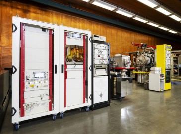
AMTC Cleanroom. Image courtesy AMTC.
Mask centers
The huge investments that are needed for the continuous improvement of mask technology lead to common R&D facilities operated by several semiconductor companies. Europe’s leading mask house Advanced Mask Technology Center (AMTC) based in Dresden/Germany was founded in 2002 by AMD, Infineon Technologies and DuPont Photomasks, which became Toppan Photomasks in 2005. Subsequently, Globalfoundries and Toppan Photomasks became the ownership partners in 2009. The company recently announced the continuation of the joint venture at least until 2017. AMTC is both a mask centre for R&D as well as a pilot production site for optical photomasks for advanced lithographic generations of 193 nm, 193 nm with immersion; and EUV. A major R&D field at the AMTC is Resolution Enhancement Technologies (RET), which allows printing features on the wafers that by now are considerably smaller than the illumination wavelength. Furthermore, AMTC’s near-term focus will be on ramping mask output for 28nm and 20nm wafer fabrication, with strategic focus on the development and introduction of 14nm optical and Extreme Ultraviolet (EUV) technologies.
EUV: the long tunnel to the light
According to Moore’s law, the number of transistors per chip doubles every two years. Extreme ultra violet lithography (EUV) is seen as the most promising manufacturing process for future generations of computer chips with feature sizes well below 16 nm. EUV uses electromagnetic radiation with a wavelength of 13.5 nm. However, large scale manufacturing with EUV masks has been delayed now for several years due to physical problems that have to be overcome under economic feasible conditions. “Extreme ultraviolet radiation is almost completely absorbed by glass substrate and in a normal atmosphere. Therefore, the processes need to be carried out under vacuum, and focusing mirrors need to be used instead of lenses. The masks are not transparent any more but reflective”, says Marc Staples, Principal Staff Manufacturing Operations at Globalfoundries in Dresden. EUV photomasks are manufactured with up to 40 different multi layers of molybdenum and silicon to make them reflective and heat absorbent. Defect control is crucial in the process of applying these layers. Staples says that the biggest challenge at the moment is the energy output of the lasers used. “What is needed is a laser output in the kw range in order to reach the targeted throughput of wafers achieved in today’s manufacturing. Here we still have a way to go.”
R&D is still double-tracked
Due to the enormous technical and financial efforts needed to make EUV competitive, the focus is still on exploitation of the potential of the traditional optical lithography with quartz masks as much as possible. Exposure methods with immersion techniques and phase-shifting photomasks such as manufactured by AMTC have expanded the conventional lithography significantly. Says Globalfoundries’ Marc Staples, ”The water layer on the wafer used in immersion lithography increases resolution and depth of focus. At 193 nm wavelength it is already standard to go to 28 nm structures in mass production. As customer demands to go further below, this is something we will definitely see and thus we are prepared to implement. However, ultimately there is no alternative to EUV.”
Written by Andreas Breyer, Senior Editor, Novus Light Technologies Today
Photos courtesy of AMTC.