


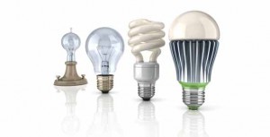


A group of researchers at Arizona State University (US) have created a new semiconductor device capable of emitting two distinct colours. As reported today in Semiconductor Science and Technology, this development could open up the possibility of using LEDs for cheap and efficient lighting.
The device takes advantage of the latest nano-scale materials and processes to emit green and red light separated by a wavelength of 97 nanometres. This bandwidth is significantly larger than a traditional semiconductor.
What is significant is that the device is much more energy efficient than traditional LEDs as the colours are emitted as lasers, meaning they emit a very sharp and specific spectral line, compared to LEDs that emit colours in a broad bandwidth.
One of the challenges in using LEDs in general lighting is that, when using semiconductors, they can emit light in a limited wavelength range, usually limited to just tens of nanometers. But for general lighting or illumination, the wavelength range needs to cover the full spectrum and should be closer to 300 nm. Single semiconductor devices can be used in a collection to cover the spectral range, but it is expensive. On the other hand, using lasers such as has been done in this study, may prove to be the key to LEDs in general lighting.
The Arizona researchers used chemical vapour deposition to create a 41 micrometer-long nanosheet made from Cadmium Sulphide and Cadmium Selenide powders, using silicon as a substrate.
Lead author of the study, Professor Cun-Zheng Ning, said: "Semiconductors are traditionally 'grown' together layer-by- layer, on an atom-scale, using the so-called epitaxial growth of crystals. Since different semiconductor crystals typically have different lattice constants, layer-by-layer growth of different semiconductors will cause defects, stress, and ultimately bad crystals, killing light emission properties."
It is because of this that current LEDs cannot have different semiconductors within them to generate red, green and blue colours for lighting.
However, nanotechnology advances allow structures such as nanowires, nanobelts and nanosheets to be grown to tolerate much larger mismatches of lattice structures, and therefore reduce defects when very different semiconductors grow together.