


Imec and PVA Tepla present results in the detection of Through Silicon via (TSV) voids in three-dimensional (3D) stacked integrated circuit (IC) technology. After having applied Scanning Acoustic Microscopy (SAM) to temporary wafer bonding/debonding inspection, they used advanced gigahertz (GHz) SAM technology to detect TSV voids at the wafer level after TSV copper (Cu) plating. Together, they will continue to investigate the applicability of high-frequency SAM for non-destructive submicron void detection.
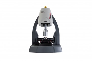
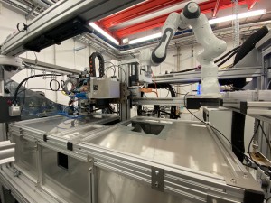
The initial focus of the collaboration was on developing metrology aimed at detecting voids after temporary wafer bonding, allowing for proper rework of 3D wafers. Temporary wafer bonding and thin wafer-handling remain challenging for 3D stacked IC technology. The development of interface particles and voids during the temporary bonding process has a detrimental impact on the subsequent wafer-thinning process steps, affecting the wafer-thinning performance as well as long-term tool stability and performance. PVA Tepla and Imec have developed an automated front opening unified pod (foup)-to-foup wafer-level process based on 200 megahertz (MHz) SAM using Tepla’s AutoWafer 300 tool. (A “foup” is a specialised plastic enclosure designed to hold silicon wafers securely and safely in a controlled environment.)

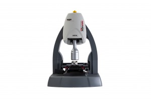
PVA Tepla AutoWafer 300
After demonstrating non-destructive detection of interface particles and voids, Imec used PVA Tepla’s high-resolution capability GHz frequency SAM tool to successfully detect voids in TSVs of 5-micrometre (µm) diameter and 50µm depth, immediately after plating. Future work will concentrate on further refining the process and implementing GHz SAM capability to increase the spatial detection resolution. Moreover, Imec and PVA Tepla will investigate the applicability of GHz SAM to detect submicron voids in TSV and to investigate other aspects related to 3D technology, such as bump connection quality.