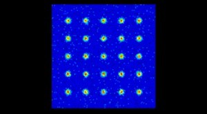
Scientific cameras have long been used to take images of various phenomena during experiments or in astrophotography. Back in the 1990s, CMOS image sensors made a groundbreaking leap by putting the detector right into the pixel. Originally developed by a team at NASA’s Jet Propulsion Lab for use in image-sensing research in space applications. By putting all of the technology on a chip, CMOS devices very quickly replaced CCD devices in scientific applications because the reduced power and size was perfect for space and scientific research. Since that time both CCD and CMOS imaging has continued to evolve, and these new technologies are what have enabled complex scientific and astronomical research.
EMCCD
While CMOS-based sensors were becoming readily available, CCD technology took a major step forward with the release of the EMCCD image sensor (or L3CCD), first developed in 2001 by Andor Technology using a detector from e2v Technologies (now Teledyne e2v) and Texas Instruments. The EMCCD is essentially a two-dimensional CCD, and it was first developed for use in astronomy. With the electron multiplying structure built onto the chip, it could detect single photon events without the need for an image intensifier.
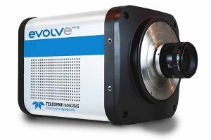
Leading camera manufacturers continue to release updated EMCCD sensors, including Teledyne Photometrics’ Evolve series.
sCMOS
The next step in the evolution of the CMOS sensor was sCMOS, first introduced in 2008 as the result of a joint development between Andor Technology, Fairchild Imaging (now part of BAE Systems), and PCO. Since its introduction, the sCMOS has gone through two more updates (Gen II in 2018 and Gen III in 2020). The advantage of the sCMOS image sensor is that it offers a large field of view and high resolution with low noise readout and high dynamic range.
While CCD and EMCCD are still used in many labs and in astronomy, sCMOS offers superior resolution, pixel pitch frame rate readout noise, dynamic range and quantum efficiency. Leading manufacturers include Andor, Hamamatsu, PCO AG, Teledyne Photometrics, Ximea among others.
For more details on sCMOS sensors, read “sCMOS Cameras Take the Scientific Imaging Stage”.
qCMOS
The latest in CMOS technology is the qCMOS (quantitative complementary metal oxide semiconductor), and what sets it apart from its predecessors is that it offers photon-number resolving technology, bringing scientific imaging to a new level.
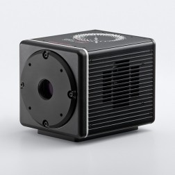
Before the release of the ORCA-Quest - currently the only qCMOS camera on the market - the lowest noise sCMOS camera was Hamamatsu's ORCA-Fusion, with a minimum readout noise of 0.7e-. The ORCA-Quest provides a readout noise value of 0.27e-, which is a reduction of more than 60%. This was the greatest challenge in designing the qCMOS, according to Dr. Sebastian Beer, Application Engineer Systems, Hamamatsu Photonics Deutschland. “When it comes to the camera, lower noise means also higher demands on the processing of the data: a very clean signal provides a very low margin for residual nonuniformities - while in sCMOS cameras those are typically hidden in the noise,” Dr. Beer said.
With all image sensors there is an optimum trade-off between resolution, sensitivity, and speed. As CMOS technology has evolved, transistor size has continued to be minimized (Moore’s Law). In addition, dark current effects and readout noise are reduced. The qCMOS technology is now able to quantify photon numbers within each pixel and this capability is enabled by extremely low noise. Dr. Beer explained that it all comes down to providing the best image possible of a given situation, namely the best signal-to-noise ratio (SNR). The SNR of a scientific image is typically influenced by the shot noise of the signal, the quantum efficiency and the noise of the sensor. Especially the noise had an important implication: if the signal was too low, it would be buried in the noise. To detect it nevertheless, a bigger signal is needed. As typically the source is limited, this means either increasing the exposure time, thus increasing sensitivity but decreasing speed. With qCMOS, however, the sensitivity hits the absolute limit of detecting and quantifying individual photons, so many of the methods to increase the signal can be performed post acquisition. While these methods are available in other cameras as well, Dr. Beer pointed out that they always increase the noise, while in qCMOS it introduces almost no excess noise.
Major distinction
The major distinction between sCMOS and qCMOS technology is the readout noise. A noise value below 0.5 e- (alongside a high digitization) allows the individual photoelectrons to become apparent in the signal, while at a level below 0.3 e-, the number of photoelectrons can be determined with a confidence of more than 90%. “Below this level of readout noise, we concluded that the sensor becomes truly quantitative, hence qCMOS,” Dr. Beer said.
At this point there are many sCMOS cameras on the market and only one qCMOS. In deciding which to choose, while the qCMOS is higher cost, it offers a very high pixel count, high speed and low dark current, which benefit certain applications such as quantum imaging. Dr Beer pointed out that sCMOS is not an option in quantum imaging, but that EMCCDs are still used due to the function of single photon counting. The difference between single photon counting in EMCCD and qCMOS is that EMCCD discriminates between 0 and 1 photons, while qCMOS has the capability to discriminate between 0, 1, 2, 3... and so on (in its current implementation up to 200). This "photon number resolving" is impossible with EMCCD, according to Dr. Beer “since anything higher than 1 photon will be detected as being one photon in single photon counting operation.”
What the future holds
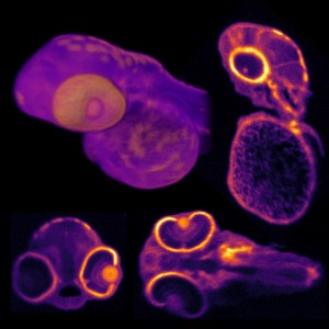
CMOS and EMCCD sensors are not going anywhere, as there are applications where they are absolutely the appropriate technology. The qCMOS camera has only been on the market a few months and is still finding applications, such as quantum imaging, but it can also be used in many other applications dealing with very low light including lightsheet imaging, super-resolution imaging, luminescence imaging and fluorescence-based assay readout. As technologies improve, application needs will become more specific and therefore drive future camera development with improvements such as native machine learning pipelines, spectral detection, special geometries and more.
Written by Anne Fischer, Editorial Director, Novus Light Technologies Today










 Back to Features